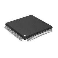
AD9882AKSTZ-100 Analog Devices Inc, AD9882AKSTZ-100 Datasheet - Page 26

AD9882AKSTZ-100
Manufacturer Part Number
AD9882AKSTZ-100
Description
IC INTERFACE/DVI 100MHZ 100LQFP
Manufacturer
Analog Devices Inc
Datasheet
1.AD9882KSTZ-100.pdf
(40 pages)
Specifications of AD9882AKSTZ-100
Applications
Video
Interface
Analog, DVI
Voltage - Supply
3.15 V ~ 3.45 V
Package / Case
100-LQFP
Mounting Type
Surface Mount
Supply Voltage Range
3.15V To 3.45V, 2.2V To 3.45V
Operating Temperature Range
0°C To +70°C
Digital Ic Case Style
LQFP
No. Of Pins
100
Msl
MSL 3 - 168 Hours
Update Rate
140MSPS
Bandwidth
300MHz
Rohs Compliant
Yes
Lead Free Status / RoHS Status
Lead free / RoHS Compliant
Available stocks
Company
Part Number
Manufacturer
Quantity
Price
Company:
Part Number:
AD9882AKSTZ-100
Manufacturer:
AD
Quantity:
1 200
Company:
Part Number:
AD9882AKSTZ-100
Manufacturer:
ADI
Quantity:
352
Company:
Part Number:
AD9882AKSTZ-100
Manufacturer:
Analog Devices Inc
Quantity:
10 000
Part Number:
AD9882AKSTZ-100
Manufacturer:
ADI/亚德诺
Quantity:
20 000
AD9882A
2-WIRE SERIAL CONTROL REGISTER DETAIL
CHIP IDENTIFICATION
0x00 7–0
An 8-bit register that represents the silicon revision.
PLL DIVIDER CONTROL
0x01 7–0
The eight most significant bits of the 12-bit PLL divide ratio
PLLDIV. (The operational divide ratio is PLLDIV + 1.)
The PLL derives a pixel clock from the incoming Hsync signal.
The pixel clock frequency is then divided by an integer value,
such that the output is phase-locked to Hsync. This PLLDIV
value determines the number of pixel times (pixels plus hori-
zontal blanking overhead) per line. This is typically 20% to 30%
more than the number of active pixels in the display.
The 12-bit value of the PLL divider supports divide ratios from
221 to 4095. The higher the value loaded in this register, the
higher the resulting clock frequency with respect to a fixed
Hsync frequency.
VESA has established some standard timing specifications that
can assist in determining the value for PLLDIV as a function of
the horizontal and vertical display resolution and frame rate
(see Table 10). However, many computer systems do not con-
form precisely to the recommendations, and these numbers
should be used only as a guide. The display system manu-
facturer should provide automatic or manual means for
optimizing PLLDIV. An incorrectly set PLLDIV usually
produces one or more vertical noise bars on the display. The
greater the error, the greater the number of bars produced.
The power-up default value of PLLDIV is 1693
(PLLDIVM = 0x69, PLLDIVL = 0xDx).
The AD9882A updates the full divide ratio only when the LSBs
are changed. Writing to this register by itself does not trigger an
update.
0x02 7–4
The four least significant bits of the 12-bit PLL divide ratio
PLLDIV. The operational divide ratio is PLLDIV + 1.
The power-up default value of PLLDIV is 1693
(PLLDIVM = 0x69, PLLDIVL = 0xDx).
The AD9882A updates the full divide ratio only when this
register is written.
Chip Revision
PLL Divide Ratio MSBs
PLL Divide Ratio LSBs
Rev. 0 | Page 26 of 40
0x03 7–6
Two bits that establish the operating range of the clock
generator. VCORNGE must be set to correspond with the
desired operating frequency (incoming pixel rate).
The PLL VCO gives the best jitter performance while operating
at high frequencies. For this reason, to output low pixel rates
and still get good jitter performance, the PLL VCO actually
operates at a higher frequency but then divides down the clock
rate afterward. Table 13 shows the pixel rates for each VCO
range setting. The PLL output divisor is automatically selected
with the VCO range setting.
Table 13. VCO Ranges
VCORNGE
00
01
10
The power-up default value is VCORNGE = 01.
0x03 5–3
Three bits that establish the current driving the loop filter in the
clock generator.
Table 14. Charge Pump Currents
Charge Pump
000
001
010
011
100
101
110
111
Charge pump must be set to correspond with the desired
operating frequency (incoming pixel rate). See Table 10 for
the charge pump current for each register setting.
The power-up default value for current is 001.
0x04 7–3
A 5-bit value that adjusts the sampling phase in 32 steps across
one pixel time. Each step represents an 11.25° shift in sampling
phase.
The power-up default phase adjust value is 0x10.
VCO Range Select
CURRENT Charge Pump Current
Phase Adjust
Pixel Rate Range
12–41
41–82
82–140
Current (µA)
50
100
150
250
350
500
750
1500


