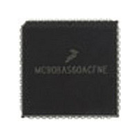
MC68HC11E0CFN3 Freescale Semiconductor, MC68HC11E0CFN3 Datasheet - Page 31

MC68HC11E0CFN3
Manufacturer Part Number
MC68HC11E0CFN3
Description
Manufacturer
Freescale Semiconductor
Datasheet
1.MC68HC11E0CFN3.pdf
(242 pages)
Specifications of MC68HC11E0CFN3
Cpu Family
HC11
Device Core Size
8b
Frequency (max)
3MHz
Interface Type
SCI/SPI
Program Memory Type
ROMLess
Program Memory Size
Not Required
Total Internal Ram Size
512Byte
# I/os (max)
38
Number Of Timers - General Purpose
8
Operating Supply Voltage (typ)
3.3/5V
Operating Supply Voltage (max)
5.5V
Operating Supply Voltage (min)
3V
On-chip Adc
8-chx8-bit
Instruction Set Architecture
CISC
Operating Temp Range
-40C to 85C
Operating Temperature Classification
Industrial
Mounting
Surface Mount
Pin Count
52
Package Type
PLCC
Lead Free Status / Rohs Status
Not Compliant
Available stocks
Company
Part Number
Manufacturer
Quantity
Price
Company:
Part Number:
MC68HC11E0CFN3
Manufacturer:
MOT
Quantity:
119
Company:
Part Number:
MC68HC11E0CFN3R2
Manufacturer:
FREESCALE
Quantity:
1 831
- Current page: 31 of 242
- Download datasheet (2Mb)
located in this ROM at $BFC0–$BFFF. The bootstrap ROM contains a small program which initializes the
serial communications interface (SCI) and allows the user to download a program into on-chip RAM. The
size of the downloaded program can be as large as the size of the on-chip RAM. After a 4-character delay,
or after receiving the character for the highest address in RAM, control passes to the loaded program at
$0000. Refer to
Use of an external pullup resistor is required when using the SCI transmitter pin because port D pins are
configured for wired-OR operation by the bootloader. In bootstrap mode, the interrupt vectors are directed
to RAM. This allows the use of interrupts through a jump table. Refer to the application note AN1060
entitled
2.3 Memory Map
The operating mode determines memory mapping and whether external addresses can be accessed.
Refer to
for each of the three families comprising the M68HC11 E series of MCUs.
Memory locations for on-chip resources are the same for both expanded and single-chip modes. Control
bits in the configuration (CONFIG) register allow EPROM and EEPROM (if present) to be disabled from
the memory map. The RAM is mapped to $0000 after reset. It can be placed at any 4-Kbyte boundary
($x000) by writing an appropriate value to the RAM and I/O map register (INIT). The 64-byte register block
is mapped to $1000 after reset and also can be placed at any 4-Kbyte boundary ($x000) by writing an
appropriate value to the INIT register. If RAM and registers are mapped to the same boundary, the first
64 bytes of RAM will be inaccessible.
Refer to
for single-chip mode only.
Freescale Semiconductor
M68HC11 Bootstrap
Figure
Figure
$D000
$FFFF
$B600
$0000
$1000
2-2,
2-7, which details the MCU register and control bit assignments. Reset states shown are
Figure
EXPANDED
Figure
EXT
EXT
2-2,
2-3,
Figure
BOOTSTRAP
Mode, that is included in this data book.
Figure 2-2. Memory Map for MC68HC11E0
Figure
2-3,
M68HC11E Family Data Sheet, Rev. 5.1
2-4,
Figure
SPECIAL
EXT
TEST
EXT
Figure
2-4,
2-5, and
Figure
2-5, and
Figure
FFC0
FFFF
BF00
BFFF
0000
01FF
1000
103F
BOOT
ROM
NORMAL
MODES
INTERRUPT
VECTORS
512 BYTES RAM
64-BYTE REGISTER BLOCK
2-6, which illustrate the memory maps
Figure
2-6.
BFC0
BFFF
SPECIAL MODES
INTERRUPT
VECTORS
Memory Map
31
Related parts for MC68HC11E0CFN3
Image
Part Number
Description
Manufacturer
Datasheet
Request
R

Part Number:
Description:
MC68HC11 EEPROM Programming from a Personal Computer
Manufacturer:
Motorola / Freescale Semiconductor
Part Number:
Description:
Manufacturer:
Freescale Semiconductor, Inc
Datasheet:
Part Number:
Description:
Manufacturer:
Freescale Semiconductor, Inc
Datasheet:
Part Number:
Description:
Manufacturer:
Freescale Semiconductor, Inc
Datasheet:
Part Number:
Description:
Manufacturer:
Freescale Semiconductor, Inc
Datasheet:
Part Number:
Description:
Manufacturer:
Freescale Semiconductor, Inc
Datasheet:
Part Number:
Description:
Manufacturer:
Freescale Semiconductor, Inc
Datasheet:
Part Number:
Description:
Manufacturer:
Freescale Semiconductor, Inc
Datasheet:
Part Number:
Description:
Manufacturer:
Freescale Semiconductor, Inc
Datasheet:
Part Number:
Description:
Manufacturer:
Freescale Semiconductor, Inc
Datasheet:
Part Number:
Description:
Manufacturer:
Freescale Semiconductor, Inc
Datasheet:
Part Number:
Description:
Manufacturer:
Freescale Semiconductor, Inc
Datasheet:
Part Number:
Description:
Manufacturer:
Freescale Semiconductor, Inc
Datasheet:
Part Number:
Description:
Manufacturer:
Freescale Semiconductor, Inc
Datasheet:
Part Number:
Description:
Manufacturer:
Freescale Semiconductor, Inc
Datasheet:


