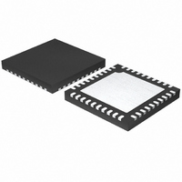
ISL6561CRZ Intersil, ISL6561CRZ Datasheet - Page 12

ISL6561CRZ
Manufacturer Part Number
ISL6561CRZ
Description
IC CTRLR PWM MULTIPHASE 40-QFN
Manufacturer
Intersil
Specifications of ISL6561CRZ
Applications
Controller, Intel VR10X
Voltage - Input
3 ~ 12 V
Number Of Outputs
4
Voltage - Output
0.84 ~ 1.6 V
Operating Temperature
0°C ~ 70°C
Mounting Type
Surface Mount
Package / Case
40-VFQFN, 40-VFQFPN
Input Voltage
12V
Output Voltage
1.65V
Supply Voltage Range
4.75V To 5.25V
Digital Ic Case Style
QFN
No. Of Pins
40
Operating Temperature Range
0°C To +70°C
Filter Terminals
SMD
Rohs Compliant
Yes
Control Mode
Voltage
Lead Free Status / RoHS Status
Lead free / RoHS Compliant
Available stocks
Company
Part Number
Manufacturer
Quantity
Price
Part Number:
ISL6561CRZ
Manufacturer:
INTERSIZ
Quantity:
20 000
Company:
Part Number:
ISL6561CRZ-T
Manufacturer:
INTERSIL
Quantity:
1 530
Company:
Part Number:
ISL6561CRZ-T
Manufacturer:
INTERSIL/PB-FREE
Quantity:
7 996
Part Number:
ISL6561CRZ-T
Manufacturer:
INTERSIL
Quantity:
20 000
Part Number:
ISL6561CRZA-T
Manufacturer:
INTERSIL
Quantity:
20 000
current. Reducing the inductor ripple current allows the
designer to use fewer or less costly output capacitors.
Another benefit of interleaving is to reduce input ripple
current. Input capacitance is determined in part by the
maximum input ripple current. Multi-phase topologies can
improve overall system cost and size by lowering input ripple
current and allowing the designer to reduce the cost of input
capacitance. The example in Figure 2 illustrates input
currents from a three-phase converter combining to reduce
the total input ripple current.
The converter depicted in Figure 2 delivers 36A to a 1.5V
load from a 12V input. The RMS input capacitor current is
5.9A. Compare this to a single-phase converter also
stepping down 12V to 1.5V at 36A. The single-phase
converter has 11.9A RMS input capacitor current. The
single-phase converter must use an input capacitor bank
with twice the RMS current capacity as the equivalent three-
phase converter.
Figures 16, 17 and 18 in the section entitled Input Capacitor
Selection can be used to determine the input-capacitor RMS
current based on load current, duty cycle, and the number of
channels. They are provided as aids in determining the
optimal input capacitor solution. Figure 19 shows the single
phase input-capacitor RMS current for comparison.
PWM Operation
The timing of each converter leg is set by the number of
active channels. The default channel setting for the ISL6561
is four. One switching cycle is defined as the time between
PWM1 pulse termination signals. The pulse termination
signal is the internally generated clock signal that triggers
the falling edge of PWM1. The cycle time of the pulse
termination signal is the inverse of the switching frequency
set by the resistor between the FS pin and ground. Each
cycle begins when the clock signal commands the channel-1
PWM output to go low. The PWM1 transition signals the
channel-1 MOSFET driver to turn off the channel-1 upper
MOSFET and turn on the channel-1 synchronous MOSFET.
In the default channel configuration, the PWM2 pulse
terminates 1/4 of a cycle after PWM1. The PWM3 output
follows another 1/4 of a cycle after PWM2. PWM4 terminates
another 1/4 of a cycle after PWM3.
If PWM3 is connected to VCC, two channel operation is
selected and the PWM2 pulse terminates 1/2 of a cycle later.
Connecting PWM4 to VCC selects three channel operation
and the pulse-termination times are spaced in 1/3 cycle
increments.
Once a PWM signal transitions low, it is held low for a
minimum of 1/3 cycle. This forced off time is required to
ensure an accurate current sample. Current sensing is
described in the next section. After the forced off time
I
L PP
,
=
(
----------------------------------------------------------- -
V
IN
–
N V
L f
S
OUT
V
IN
) V
OUT
12
(EQ. 2)
ISL6561
expires, the PWM output is enabled. The PWM output state
is driven by the position of the error amplifier output signal,
V
sawtooth ramp as illustrated in Figure 4. When the modified
V
transitions high. The MOSFET driver detects the change in
state of the PWM signal, turns off the synchronous MOSFET
and turns on the upper MOSFET. The PWM signal remains
high until the pulse termination signal commands the
beginning of the next cycle by triggering the PWM signal low.
Current Sensing
The ISL6561 supports inductor DCR sensing or MOSFET
r
and 5, represents channel n of an N-channel converter. This
circuitry is repeated for each channel in the converter, but
may not be active depending on the status of the PWM3 and
PWM4 pins, as described in the PWM Operation section.
MOSFET r
The controller can sense the channel load current by
sampling the voltage across the lower MOSFET r
in Figure 6. The amplifier is ground-reference by connecting
the ISEN- input to the source of the lower MOSFET. ISEN+
connects to the PHASE node through a resistor R
voltage across R
across the r
conducting. The resulting current into the ISEN+ pin is
proportional to the channel current I
then sampled and held after sufficient settling time as
described in current sampling section. The sampled current
I
and overcurrent protection. From Figure 4, the following
equation for I
where I
I
n
DS(ON)
SEN
COMP
COMP
, is used for channel-current balance, load-line regulation,
FIGURE 3. MOSFET r
SAMPLE
HOLD
=
ISL6561 INTERNAL CIRCUIT
, minus the current correction signal relative to the
I
&
L
n
I
voltage crosses the sawtooth ramp, the PWM output
sensing. The internal circuitry, shown in Figures 3
L
I
is the channel current.
SEN
r
----------------------
DS(ON)
DS ON
R
DS(ON)
ISEN
SEN
(
=
I L
ISEN
)
is derived
r DS ON
------------------------- -
Sensing
+
-
R
of the lower MOSFET while it is
ISEN
(
is equivalent to the voltage drop
DS(ON)
)
ISEN+(n)
ISEN-(n)
CURRENT-SENSING CIRCUIT
EXTERNAL CIRCUIT
R
(PTC)
ISEN
L
. The ISEN current is
V
IN
+
-
I
L
N-CHANNEL
MOSFETs
r
DS ON
I
DS(ON)
L
ISEN
(
May 12, 2005
FN9098.5
(EQ. 3)
)
. The
as


