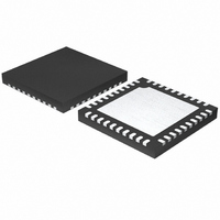
ISL6561CRZ Intersil, ISL6561CRZ Datasheet - Page 14

ISL6561CRZ
Manufacturer Part Number
ISL6561CRZ
Description
IC CTRLR PWM MULTIPHASE 40-QFN
Manufacturer
Intersil
Specifications of ISL6561CRZ
Applications
Controller, Intel VR10X
Voltage - Input
3 ~ 12 V
Number Of Outputs
4
Voltage - Output
0.84 ~ 1.6 V
Operating Temperature
0°C ~ 70°C
Mounting Type
Surface Mount
Package / Case
40-VFQFN, 40-VFQFPN
Input Voltage
12V
Output Voltage
1.65V
Supply Voltage Range
4.75V To 5.25V
Digital Ic Case Style
QFN
No. Of Pins
40
Operating Temperature Range
0°C To +70°C
Filter Terminals
SMD
Rohs Compliant
Yes
Control Mode
Voltage
Lead Free Status / RoHS Status
Lead free / RoHS Compliant
Available stocks
Company
Part Number
Manufacturer
Quantity
Price
Part Number:
ISL6561CRZ
Manufacturer:
INTERSIZ
Quantity:
20 000
Company:
Part Number:
ISL6561CRZ-T
Manufacturer:
INTERSIL
Quantity:
1 530
Company:
Part Number:
ISL6561CRZ-T
Manufacturer:
INTERSIL/PB-FREE
Quantity:
7 996
Part Number:
ISL6561CRZ-T
Manufacturer:
INTERSIL
Quantity:
20 000
Part Number:
ISL6561CRZA-T
Manufacturer:
INTERSIL
Quantity:
20 000
Channel current balance is essential in realizing the thermal
advantage of multi-phase operation. The heat generated in
down converting is dissipated over multiple devices and a
greater area. The designer avoids the complexity of driving
multiple parallel MOSFETs, and the expense of using heat
sinks and nonstandard magnetic materials.
Voltage Regulation
The integrating compensation network shown in Figure 7
assures that the steady-state error in the output voltage is
limited only to the error in the reference voltage (output of
the DAC) and offset errors in the OFS current source,
remote-sense and error amplifiers. Intersil specifies the
guaranteed tolerance of the ISL6561 to include the
combined tolerances of each of these elements.
The output of the error amplifier, V
sawtooth waveform to generate the PWM signals. The PWM
signals control the timing of the Intersil MOSFET drivers and
regulate the converter output to the specified reference
voltage. The internal and external circuitry that controls
voltage regulation is illustrated in Figure 7.
FIGURE 7. OUTPUT VOLTAGE AND LOAD-LINE
FIGURE 6. CHANNEL-1 PWM FUNCTION AND CURRENT-
R
FB
V
COMP
V
V
EXTERNAL CIRCUIT
OUT
OUT
+
-
V
FILTER
DROOP
C
R
REF
+
-
C
BALANCE ADJUSTMENT
REGULATION WITH OFFSET ADUJUSTMENT
R
C
REF
+
I
ER
C
-
+
IDROOP
f(jω)
I
1
COMP
VDIFF
RGND
VSEN
DAC
REF
-
FB
I
AVG
SAWTOOTH SIGNAL
NOTE: *Channels 3 and 4 are optional.
14
÷
ISL6561 INTERNAL CIRCUIT
N
I
AVG
COMP
+
-
DIFFERENTIAL
REMOTE-SENSE
AMPLIFIER
ERROR AMPLIFIER
, is compared to the
+
-
Σ
+
-
V
COMP
PWM1
I
I
I
4
3
2
*
*
ISL6561
The ISL6561 incorporates an internal differential remote-
sense amplifier in the feedback path. The amplifier removes
the voltage error encountered when measuring the output
voltage relative to the local controller ground reference point
resulting in a more accurate means of sensing output
voltage. Connect the microprocessor sense pins to the non-
inverting input, VSEN, and inverting input, RGND, of the
remote-sense amplifier. The remote-sense output, V
connected to the inverting input of the error amplifier through
an external resistor.
A digital to analog converter (DAC) generates a reference
voltage based on the state of logic signals at pins VID4
through VID12.5. The DAC decodes the a 6-bit logic signal
(VID) into one of the discrete voltages shown in Table 1.
Each VID input offers a 50µA pull-up to an internal 2.5V
source for use with open-drain outputs. The pull-up current
diminishes to zero above the logic threshold to protect
voltage-sensitive output devices. External pull-up resistors
can augment the pull-up current sources in case leakage
into the driving device is greater than 50µA.
Load-Line Regulation
Some microprocessor manufacturers require a precisely-
controlled output resistance. This dependence of output
voltage on load current is often termed “droop” or “load line”
regulation. By adding a well controlled output impedance,
the output voltage can effectively be level shifted in a
direction which works to achieve the load-line regulation
required by these manufacturers.
VID4
0
0
0
0
0
0
0
0
0
0
0
0
0
0
0
0
0
0
TABLE 1. VOLTAGE IDENTIFICATION (VID) CODES
VID3
1
1
1
1
1
0
0
0
0
0
0
0
0
0
0
0
0
0
VID2
0
0
0
0
0
1
1
1
1
1
1
1
1
0
0
0
0
0
VID1
1
0
0
0
0
1
1
1
1
0
0
0
0
1
1
1
1
0
VID0
0
1
1
0
0
1
1
0
0
1
1
0
0
1
1
0
0
1
VID12.5
0
1
0
1
0
1
0
1
0
1
0
1
0
1
0
1
0
1
0.8375V
0.8500V
0.8625V
0.8750V
0.8875V
0.9000V
0.9125V
0.9250V
0.9375V
0.9500V
0.9625V
0.975V0
0.9875V
1.0000V
1.0125V
1.0375V
1.0500V
1.0250v
May 12, 2005
VDAC
DIFF
FN9098.5
, is


