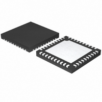
ISL6561CRZ Intersil, ISL6561CRZ Datasheet - Page 16

ISL6561CRZ
Manufacturer Part Number
ISL6561CRZ
Description
IC CTRLR PWM MULTIPHASE 40-QFN
Manufacturer
Intersil
Specifications of ISL6561CRZ
Applications
Controller, Intel VR10X
Voltage - Input
3 ~ 12 V
Number Of Outputs
4
Voltage - Output
0.84 ~ 1.6 V
Operating Temperature
0°C ~ 70°C
Mounting Type
Surface Mount
Package / Case
40-VFQFN, 40-VFQFPN
Input Voltage
12V
Output Voltage
1.65V
Supply Voltage Range
4.75V To 5.25V
Digital Ic Case Style
QFN
No. Of Pins
40
Operating Temperature Range
0°C To +70°C
Filter Terminals
SMD
Rohs Compliant
Yes
Control Mode
Voltage
Lead Free Status / RoHS Status
Lead free / RoHS Compliant
Available stocks
Company
Part Number
Manufacturer
Quantity
Price
Part Number:
ISL6561CRZ
Manufacturer:
INTERSIZ
Quantity:
20 000
Company:
Part Number:
ISL6561CRZ-T
Manufacturer:
INTERSIL
Quantity:
1 530
Company:
Part Number:
ISL6561CRZ-T
Manufacturer:
INTERSIL/PB-FREE
Quantity:
7 996
Part Number:
ISL6561CRZ-T
Manufacturer:
INTERSIL
Quantity:
20 000
Part Number:
ISL6561CRZA-T
Manufacturer:
INTERSIL
Quantity:
20 000
between DAC and REF, R
(I
functions are shown in Figures 8.
As evident in Figure 8, the OFSOUT pin must be connected
to the REF pin for this current injection to function in
ISL6561CR. The current flowing through R
offset at the REF pin, which is ultimately duplicated at the
output of the regulator.
Once the desired output offset voltage has been determined,
use the following formulas to set R
For Positive Offset (connect R
For Negative Offset (connect R
Dynamic VID
Modern microprocessors need to make changes to their
core voltage as part of normal operation. They direct the
core-voltage regulator to do this by making changes to the
VID inputs during regulator operation. The power
management solution is required to monitor the DAC inputs
and respond to on-the-fly VID changes in a controlled
R
R
OFS
OFS
OFS
FIGURE 8. OUTPUT VOLTAGE OFFSET PROGRAMMING
x R
=
=
0.5
----------------------------- -
--------------------------
V
2
REF
V
2.0V
OFFSET
×
OFFSET
×
R
WITH ISL6561CR
) is equal to the desired offset voltage. These
VCC
R
+
REF
-
REF
0.5V
E/A
GND
+
-
REF
FB
16
, is selected so that the product
OFS
OFS
OFS
to VCC):
DYNAMIC
to GND):
VID D/A
:
ISL6561CR
REF
creates an
DAC
REF
OFS
GND
VCC
or
(EQ. 10)
(EQ. 11)
R
R
REF
OFS
ISL6561
manner. Supervising the safe output voltage transition within
the DAC range of the processor without discontinuity or
disruption is a necessary function of the core-voltage
regulator.
The ISL6561 checks the VID inputs six times every switching
cycle. If the VID code is found to have has changed, the
controller waits half of a complete cycle before executing a
12.5mV change. If during the half-cycle wait period, the
difference between DAC level and the new VID code
changes, no change is made. If the VID code is more than 1
bit higher or lower than the DAC (not recommended), the
controller will execute 12.5mV changes six times per cycle
until VID and DAC are equal. It is for this reason that it is
important to carefully control the rate of VID stepping in 1-bit
increments.
In order to ensure the smooth transition of output voltage
during VID change, a VID step change smoothing network
composed of R
based voltage regulator. The selection of R
the desired offset as detailed above in Output-Voltage Offset
Programming. The selection of C
duration for 1 bit VID change and the allowable delay time.
Assuming the microprocessor controls the VID change at 1
bit every T
R
Typically R
change rate of 5µs per bit, the value of C
on Equation 12.
Temperature Compensation
Both the MOSFET r
vary in proportion to varying temperature. This means that a
circuit using r
subject to a corresponding error in current measurement. In
order to compensate for this temperature-related error, a
temperature compensation circuit is provided within
ISL6561. This circuit senses the internal IC temperature and,
based on a resistor-selectable scaling factor, adjust the
droop current ouput to the IDROOP pin. When the TCOMP
resistor is properly selected, the droop current can
accurately represent the load current to achieve a linear,
temperature-independant load line.
The value of the Tcomp resistor can be determined using
Equation 13.
In Equation 13, K
between the ISL6561 and the lower MOSFET or output
inductor. It represents how closely the controller temperature
C
R
REF
REF
TCOMP
and C
R
REF
=
VID
REF
--------------------- -
REF
K
=
DS(ON)
, the relationship between the time constant of
T
4 T
α
REF
K
is selected to be 1kΩ, so with a VID step
network and T
TC
T
VID
is the temperature coupling coefficient
and C
DS(ON)
or DCR to sense channel current is
REF
and inductor DCR of inductor
is required for an ISL6561
VID
REF
is given by Equation 12.
is based on the time
REF
REF
is 22nF based
is based on
May 12, 2005
(EQ. 12)
(EQ. 13)
FN9098.5


