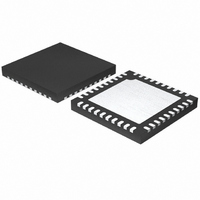
ISL6561CRZ Intersil, ISL6561CRZ Datasheet - Page 23

ISL6561CRZ
Manufacturer Part Number
ISL6561CRZ
Description
IC CTRLR PWM MULTIPHASE 40-QFN
Manufacturer
Intersil
Specifications of ISL6561CRZ
Applications
Controller, Intel VR10X
Voltage - Input
3 ~ 12 V
Number Of Outputs
4
Voltage - Output
0.84 ~ 1.6 V
Operating Temperature
0°C ~ 70°C
Mounting Type
Surface Mount
Package / Case
40-VFQFN, 40-VFQFPN
Input Voltage
12V
Output Voltage
1.65V
Supply Voltage Range
4.75V To 5.25V
Digital Ic Case Style
QFN
No. Of Pins
40
Operating Temperature Range
0°C To +70°C
Filter Terminals
SMD
Rohs Compliant
Yes
Control Mode
Voltage
Lead Free Status / RoHS Status
Lead free / RoHS Compliant
Available stocks
Company
Part Number
Manufacturer
Quantity
Price
Part Number:
ISL6561CRZ
Manufacturer:
INTERSIZ
Quantity:
20 000
Company:
Part Number:
ISL6561CRZ-T
Manufacturer:
INTERSIL
Quantity:
1 530
Company:
Part Number:
ISL6561CRZ-T
Manufacturer:
INTERSIL/PB-FREE
Quantity:
7 996
Part Number:
ISL6561CRZ-T
Manufacturer:
INTERSIL
Quantity:
20 000
Part Number:
ISL6561CRZA-T
Manufacturer:
INTERSIL
Quantity:
20 000
voltage deviation is less than the allowable maximum.
Neglecting the contribution of inductor current and regulator
response, the output voltage initially deviates by an amount
The filter capacitor must have sufficiently low ESL and ESR
so that ∆V < ∆V
Most capacitor solutions rely on a mixture of high-frequency
capacitors with relatively low capacitance in combination
with bulk capacitors having high capacitance but limited
high-frequency performance. Minimizing the ESL of the high-
frequency capacitors allows them to support the output
voltage as the current increases. Minimizing the ESR of the
bulk capacitors allows them to supply the increased current
with less output voltage deviation.
The ESR of the bulk capacitors also creates the majority of
the output-voltage ripple. As the bulk capacitors sink and
source the inductor ac ripple current (see Interleaving and
Equation 2), a voltage develops across the bulk-capacitor
ESR equal to I
are selected, the maximum allowable ripple voltage,
V
Since the capacitors are supplying a decreasing portion of
the load current while the regulator recovers from the
transient, the capacitor voltage becomes slightly depleted.
The output inductors must be capable of assuming the entire
load current before the output voltage decreases more than
∆V
Equation 29 gives the upper limit on L for the cases when the
trailing edge of the current transient causes a greater output-
voltage deviation than the leading edge. Equation 30
addresses the leading edge. Normally, the trailing edge
dictates the selection of L because duty cycles are usually
less than 50%. Nevertheless, both inequalities should be
evaluated, and L should be selected based on the lower of
the two results. In each equation, L is the per-channel
inductance, C is the total output capacitance, and N is the
number of active channels.
∆V
L
L
L
PP(MAX)
≤
≤
≥
MAX
≈
2NCV
-------------------- - ∆V
(
------------------------- - ∆V
(
1.25
(
ESR
(
(
ESL
∆I
∆I
. This places an upper limit on inductance.
)
) NC
2
)
O
2
)
, determines the lower limit on the inductance.
)
----------------------------------------------------------- -
di
---- -
dt
V
IN
+
f
S
C,PP
MAX
(
MAX
V
–
ESR
MAX
IN
N V
V
–
(ESR). Thus, once the output capacitors
.
OUT
PP MAX
) ∆I
–
∆I ESR
∆I ESR
(
(
V
(
OUT
)
)
23
)
V
IN
–
V
O
(EQ. 27)
(EQ. 28)
(EQ. 29)
(EQ. 30)
ISL6561
Input Supply Voltage Selection
The VCC input of the ISL6561 can be connected either
directly to a +5V supply or through a current limiting resistor
to a +12V supply. An integrated 5.8V shunt regulator
maintains the voltage on the VCC pin when a +12V supply is
used. A 300Ω resistor is suggested for limiting the current
into the VCC pin to a worst-case maximum of approximately
25mA.
Switching Frequency
There are a number of variables to consider when choosing
the switching frequency, as there are considerable effects on
the upper-MOSFET loss calculation. These effects are
outlined in MOSFETs, and they establish the upper limit for
the switching frequency. The lower limit is established by the
requirement for fast transient response and small output-
voltage ripple as outlined in Output Filter Design. Choose the
lowest switching frequency that allows the regulator to meet
the transient-response requirements.
Switching frequency is determined by the selection of the
frequency-setting resistor, R
Typical Application on pages 3 and 6). Figure 15 and
Equation 31 are provided to assist in selecting the correct
value for R
Input Capacitor Selection
The input capacitors are responsible for sourcing the ac
component of the input current flowing into the upper
MOSFETs. Their RMS current capacity must be sufficient to
handle the ac component of the current drawn by the upper
MOSFETs which is related to duty cycle and the number of
active phases.
R
T
1000
100
=
10
1.0203 10
10
FIGURE 15. R
T
.
(
)
[
10.6258- 1.03167
SWITCHING FREQUENCY (kHz)
T
100
vs SWITCHING FREQUENCY
(
·
T
(see the figures labeled
)
log
( )
f
S
]
–
1000
1200
May 12, 2005
(EQ. 31)
FN9098.5
10000


