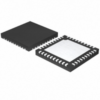
ISL6561CRZ Intersil, ISL6561CRZ Datasheet - Page 19

ISL6561CRZ
Manufacturer Part Number
ISL6561CRZ
Description
IC CTRLR PWM MULTIPHASE 40-QFN
Manufacturer
Intersil
Specifications of ISL6561CRZ
Applications
Controller, Intel VR10X
Voltage - Input
3 ~ 12 V
Number Of Outputs
4
Voltage - Output
0.84 ~ 1.6 V
Operating Temperature
0°C ~ 70°C
Mounting Type
Surface Mount
Package / Case
40-VFQFN, 40-VFQFPN
Input Voltage
12V
Output Voltage
1.65V
Supply Voltage Range
4.75V To 5.25V
Digital Ic Case Style
QFN
No. Of Pins
40
Operating Temperature Range
0°C To +70°C
Filter Terminals
SMD
Rohs Compliant
Yes
Control Mode
Voltage
Lead Free Status / RoHS Status
Lead free / RoHS Compliant
Available stocks
Company
Part Number
Manufacturer
Quantity
Price
Part Number:
ISL6561CRZ
Manufacturer:
INTERSIZ
Quantity:
20 000
Company:
Part Number:
ISL6561CRZ-T
Manufacturer:
INTERSIL
Quantity:
1 530
Company:
Part Number:
ISL6561CRZ-T
Manufacturer:
INTERSIL/PB-FREE
Quantity:
7 996
Part Number:
ISL6561CRZ-T
Manufacturer:
INTERSIL
Quantity:
20 000
Part Number:
ISL6561CRZA-T
Manufacturer:
INTERSIL
Quantity:
20 000
command the lower MOSFETs to turn on. The ISL6561 will
continue to protect the load in this fashion as long as the
overvoltage condition recurs.
Simultaneous to the protective action of the PWM outputs,
the OVP pin pulls to VCC delivering up to 100mA to the gate
of a crowbar MOSFET or SCR placed either on the input rail
or the output rail. Turning on the MOSFET or SCR collapses
the power rail and causes a fuse placed further up stream to
blow. The fuse must be sized such that the MOSFET or SCR
will not overheat before the fuse blows. The OVP pin is
tolerant to 12V (see Absolute Maximum Ratings), so an
external resistor pull up can be used to augment the driving
capability. If using a pull up resistor in conjunction with the
internal overvoltage protection function, care must be taken
to avoid nuisance trips that could occur when VCC is below
2V. In that case, the controller is incapable of holding OVP
low.
Once an overvoltage condition is detected, normal PWM
operation ceases until the ISL6561 is reset. Cycling the
voltage on EN or ENLL or VCC below the POR-falling
threshold will reset the controller. Cycling the VID codes will
not reset the controller.
Overcurrent Protection
ISL6561 has two levels of overcurrent protection. Each
phase is protected from a sustained overcurrent condition on
a delayed basis, while the combined phase currents are
protected on an instantaneous basis.
In instantaneous protection mode, the ISL6561 takes
advantage of the proportionality between the load current
and the average current, I
condition. See the Channel-Current Balance section for
more detail on how the average current is measured. The
average current is continually compared with a constant
100µA reference current as shown in Figure 11. Once the
average current exceeds the reference current, a comparator
triggers the converter to shutdown.
FIGURE 12. OVERCURRENT BEHAVIOR IN HICCUP MODE.
0A
0V
OUTPUT CURRENT, 50A/DIV
OUTPUT VOLTAGE,
500mV/DIV
F
SW
= 500kHz
AVG
2ms/DIV
19
to detect an overcurrent
ISL6561
In individual overcurrent protection mode, the ISL6561
continuously compares the current of each channel with the
same 100µA reference current. If any channel current
exceeds the reference current continuously for eight
consecutive cycles, the comparator triggers the converter to
shutdown.
At the beginning of overcurrent shutdown, the controller
places all PWM signals in a high-impedance state
commanding the Intersil MOSFET driver ICs to turn off both
upper and lower MOSFETs. The system remains in this
state a period of 4096 switching cycles. If the controller is still
enabled at the end of this wait period, it will attempt a soft
start. If the fault remains, trip-retry cycles continue
indefinitely (as shown in Figure 12) until either controller is
disabled or the fault is cleared. Note that the energy
delivered during trip-retry cycling is much less than during
full-load operation, so there, there is no thermal hazard
during this kind of operation.
General Design Guide
This design guide is intended to provide a high-level
explanation of the steps necessary to create a multi-phase
power converter. It is assumed that the reader is familiar with
many of the basic skills and techniques referenced below. In
addition to this guide, Intersil provides complete reference
designs that include schematics, bills of materials, and
example board layouts for all common microprocessor
applications.
Power Stages
The first step in designing a multi-phase converter is to
determine the number of phases. This determination
depends heavily on the cost analysis which in turn depends
on system constraints that differ from one design to the next.
Principally, the designer will be concerned with whether
components can be mounted on both sides of the circuit
board; whether through-hole components are permitted; and
the total board space available for power-supply circuitry.
Generally speaking, the most economical solutions are
those in which each phase handles between 15 and 20A. All
surface-mount designs will tend toward the lower end of this
current range. If through-hole MOSFETs and inductors can
be used, higher per-phase currents are possible. In cases
where board space is the limiting constraint, current may be
pushed above 30A per phase, but these designs require
heat sinks and forced air to cool the MOSFETs, inductors
and heat-dissipating surfaces.
MOSFETs
The choice of MOSFETs depends on the current each
MOSFET will be required to conduct; the switching frequency;
the capability of the MOSFETs to dissipate heat; and the
availability and nature of heat sinking and air flow.
May 12, 2005
FN9098.5


