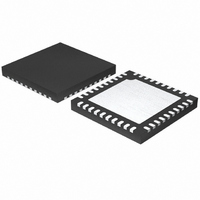
ISL6561CRZ Intersil, ISL6561CRZ Datasheet - Page 15

ISL6561CRZ
Manufacturer Part Number
ISL6561CRZ
Description
IC CTRLR PWM MULTIPHASE 40-QFN
Manufacturer
Intersil
Specifications of ISL6561CRZ
Applications
Controller, Intel VR10X
Voltage - Input
3 ~ 12 V
Number Of Outputs
4
Voltage - Output
0.84 ~ 1.6 V
Operating Temperature
0°C ~ 70°C
Mounting Type
Surface Mount
Package / Case
40-VFQFN, 40-VFQFPN
Input Voltage
12V
Output Voltage
1.65V
Supply Voltage Range
4.75V To 5.25V
Digital Ic Case Style
QFN
No. Of Pins
40
Operating Temperature Range
0°C To +70°C
Filter Terminals
SMD
Rohs Compliant
Yes
Control Mode
Voltage
Lead Free Status / RoHS Status
Lead free / RoHS Compliant
Available stocks
Company
Part Number
Manufacturer
Quantity
Price
Part Number:
ISL6561CRZ
Manufacturer:
INTERSIZ
Quantity:
20 000
Company:
Part Number:
ISL6561CRZ-T
Manufacturer:
INTERSIL
Quantity:
1 530
Company:
Part Number:
ISL6561CRZ-T
Manufacturer:
INTERSIL/PB-FREE
Quantity:
7 996
Part Number:
ISL6561CRZ-T
Manufacturer:
INTERSIL
Quantity:
20 000
Part Number:
ISL6561CRZA-T
Manufacturer:
INTERSIL
Quantity:
20 000
TABLE 1. VOLTAGE IDENTIFICATION (VID) CODES (Continued)
VID4
0
0
0
1
1
1
1
1
1
1
1
1
1
1
1
1
1
1
1
1
1
1
1
1
1
1
1
1
1
1
1
1
1
1
1
0
0
0
0
0
VID3
0
0
0
1
1
1
1
1
1
1
1
1
1
1
1
1
1
1
1
0
0
0
0
0
0
0
0
0
0
0
0
0
0
0
0
1
1
1
1
1
VID2
0
0
0
1
1
1
1
1
1
1
1
0
0
0
0
0
0
0
0
1
1
1
1
1
1
1
1
0
0
0
0
0
0
0
0
1
1
1
1
1
VID1
0
0
0
1
1
1
1
0
0
0
0
1
1
1
1
0
0
0
0
1
1
1
1
0
0
0
0
1
1
1
1
0
0
0
0
1
1
1
1
0
15
VID0
1
0
0
1
1
0
0
1
1
0
0
1
1
0
0
1
1
0
0
1
1
0
0
1
1
0
0
1
1
0
0
1
1
0
0
1
1
0
0
1
VID12.5
0
1
0
1
0
1
0
1
0
1
0
1
0
1
0
1
0
1
0
1
0
1
0
1
0
1
0
1
0
1
0
1
0
1
0
1
0
1
0
1
1.0625V
1.0750V
1.0875V
1.1000V
1.1125V
1.1250V
1.1375V
1.1500V
1.1625V
1.1750V
1.1875V
1.2000V
1.2125V
1.2250V
1.2475V
1.2500V
1.2625V
1.2750V
1.2875V
1.3000V
1.3125V
1.3250V
1.3375V
1.3500V
1.3625V
1.3750V
1.3875V
1.4000V
1.4125V
1.4250V
1.4375V
1.4500V
1.4625V
1.4750V
1.4875V
1.5000V
1.5125V
1.5250V
VDAC
OFF
OFF
ISL6561
In other cases, the designer may determine that a more
cost-effective solution can be achieved by adding droop.
Droop can help to control the output-voltage spike that
results from fast load-current demand changes.
The magnitude of the spike is dictated by the ESR and ESL
of the output capacitors selected. By positioning the no-load
voltage level near the upper specification limit, a larger
negative spike can be sustained without crossing the lower
limit. By adding a well controlled output impedance, the
output voltage under load can effectively be level shifted
down so that a larger positive spike can be sustained without
crossing the upper specification limit.
As shown in Figure 8, a current proportional to the average
current in all active channels, I
load-line regulation resistor, R
across R
creating an output voltage droop with a steady-state value
defined as
The regulated output voltage is reduced by the droop voltage
V
derived by combining Equations 8 with the appropriate
sample current expression defined by the current sense
method employed.
Where V
programmed offset voltage, V
of the converter, R
and R
r
Output-Voltage Offset Programming
The ISL6561 allows the designer to accurately adjust the
offset voltage. When a resistor, R
OFS and VCC, the voltage across it is regulated to 2.0V. This
causes a proportional current (I
R
regulated to 0.5V, and I
V
V
DS(ON)
TABLE 1. VOLTAGE IDENTIFICATION (VID) CODES (Continued)
DROOP
OUT
OFS
VID4
DROOP
0
0
0
0
0
0
FB
is connected to ground, the voltage across it is
=
, or R
. The output voltage as a function of load current is
V
REF
FB
is the feedback resistor. R
VID3
=
REF
1
1
1
1
1
1
I
is proportional to the output current, effectively
AVG
is the reference voltage, V
SENSE
–
V
VID2
R
OFFSET
ISEN
1
1
1
0
0
0
FB
depending on the sensing method.
OFS
is the sense resistor in the ISEN line,
VID1
–
0
0
0
1
1
1
I
-------------
flows out of OFS. A resistor
OUT
OUT
4
FB
AVG
OFS
VID0
. The resulting voltage drop
OFS
----------------- - R
R
1
0
0
1
1
0
is the total output current
, flows from FB through a
ISEN
R
X
) to flow into OFS. If
X
, is connected between
has a value of DCR,
OFS
VID12.5
FB
0
1
0
1
0
1
is the
1.5375V
1.5500V
1.5625V
1.5750V
1.5875V
May 12, 2005
1.600V
VDAC
FN9098.5
(EQ. 8)
(EQ. 9)


