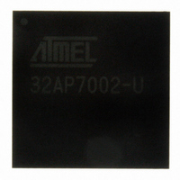
AT32AP7002-CTUT Atmel, AT32AP7002-CTUT Datasheet - Page 179

AT32AP7002-CTUT
Manufacturer Part Number
AT32AP7002-CTUT
Description
IC MCU 32BIT AVR32 196-CBGA
Manufacturer
Atmel
Series
AVR®32 AP7r
Specifications of AT32AP7002-CTUT
Core Processor
AVR
Core Size
32-Bit
Speed
150MHz
Connectivity
EBI/EMI, I²C, MMC, PS2, SPI, SSC, UART/USART, USB
Peripherals
AC'97, DMA, I²C, LCD, POR, PWM, WDT
Number Of I /o
85
Program Memory Type
ROMless
Ram Size
32K x 8
Voltage - Supply (vcc/vdd)
1.65 V ~ 1.95 V
Data Converters
D/A 2x16b
Oscillator Type
Internal
Operating Temperature
-40°C ~ 85°C
Package / Case
196-CBGA
Data Bus Width
32 bit
Data Ram Size
32 KB
Interface Type
I2C, JTAG, PS2, SPI, SSC, UART, USART, USB
Maximum Clock Frequency
150 MHz
Number Of Timers
3
Maximum Operating Temperature
+ 85 C
Mounting Style
SMD/SMT
Minimum Operating Temperature
- 40 C
On-chip Dac
16 bit, 2 Channel
Package
196CTBGA
Device Core
AVR32
Family Name
AT32
Maximum Speed
150 MHz
Operating Supply Voltage
1.8|3.3 V
For Use With
ATAVRONEKIT - KIT AVR/AVR32 DEBUGGER/PROGRMMRATNGW100 - KIT AVR32 NETWORK GATEWAYATSTK1000 - KIT STARTER FOR AVR32AP7000
Lead Free Status / RoHS Status
Lead free / RoHS Compliant
Eeprom Size
-
Program Memory Size
-
Lead Free Status / Rohs Status
Details
Available stocks
Company
Part Number
Manufacturer
Quantity
Price
- Current page: 179 of 896
- Download datasheet (13Mb)
17.10.1.2
32054F–AVR32–09/09
Multi-block Transfer with Linked List for Source and Linked List for Destination (Row 10)
4. After the DMACA selected channel has been programmed, enable the channel by writing
5. Source and destination request single and burst DMA transactions to transfer the block of
6. Once the transfer completes, hardware sets the interrupts and disables the channel. At
1. Read the Channel Enable register to choose a free (disabled) channel.
2. Set up the chain of Linked List Items (otherwise known as block descriptors) in memory.
3. Write the channel configuration information into the CFGx register for channel x.
– ii. Set up the transfer characteristics, such as:
e. Write the channel configuration information into the CFGx register for channel x.
– i. Designate the handshaking interface type (hardware or software) for the source and
– ii. If the hardware handshaking interface is activated for the source or destination
a ‘1’ to the ChEnReg.CH_EN bit. Make sure that bit 0 of the DmaCfgReg register is
enabled.
data (assuming non-memory peripherals). The DMACA acknowledges at the completion
of every transaction (burst and single) in the block and carry out the block transfer.
this time you can either respond to the Block Complete or Transfer Complete interrupts,
or poll for the Channel Enable (ChEnReg.CH_EN) bit until it is cleared by hardware, to
detect when the transfer is complete.
Write the control information in the LLI.CTLx register location of the block descriptor for
each LLI in memory (see
register, you can program the following:
a. Set up the transfer type (memory or non-memory peripheral for source and destina-
b. Set up the transfer characteristics, such as:
– i. Transfer width for the source in the SRC_TR_WIDTH field.
– ii. Transfer width for the destination in the DST_TR_WIDTH field.
– iii. Source master layer in the SMS field where source resides.
– iv. Destination master layer in the DMS field where destination resides.
– v. Incrementing/decrementing or fixed address for source in SINC field.
– vi. Incrementing/decrementing or fixed address for destination DINC field.
a. Designate the handshaking interface type (hardware or software) for the source and
destination peripherals. This is not required for memory. This step requires
programming the HS_SEL_SRC/HS_SEL_DST bits, respectively. Writing a ‘0’
activates the hardware handshaking interface to handle source/destination requests.
Writing a ‘1’ activates the software handshaking interface to handle source/destination
requests.
peripheral, assign a handshaking interface to the source and destination peripheral.
This requires programming the SRC_PER and DEST_PER bits, respectively.
tion) and flow control device by programming the TT_FC of the CTLx register.
destination peripherals. This is not required for memory. This step requires program-
– Transfer width for the source in the SRC_TR_WIDTH field.
– Transfer width for the destination in the DST_TR_WIDTH field.
– Source master layer in the SMS field where source resides.
– Destination master layer in the DMS field where destination resides.
– Incrementing/decrementing or fixed address for source in SINC field.
– Incrementing/decrementing or fixed address for destination in DINC field.
Figure 17-7 on page
175) for channel x. For example, in the
AT32AP7002
179
Related parts for AT32AP7002-CTUT
Image
Part Number
Description
Manufacturer
Datasheet
Request
R

Part Number:
Description:
DEV KIT FOR AVR/AVR32
Manufacturer:
Atmel
Datasheet:

Part Number:
Description:
INTERVAL AND WIPE/WASH WIPER CONTROL IC WITH DELAY
Manufacturer:
ATMEL Corporation
Datasheet:

Part Number:
Description:
Low-Voltage Voice-Switched IC for Hands-Free Operation
Manufacturer:
ATMEL Corporation
Datasheet:

Part Number:
Description:
MONOLITHIC INTEGRATED FEATUREPHONE CIRCUIT
Manufacturer:
ATMEL Corporation
Datasheet:

Part Number:
Description:
AM-FM Receiver IC U4255BM-M
Manufacturer:
ATMEL Corporation
Datasheet:

Part Number:
Description:
Monolithic Integrated Feature Phone Circuit
Manufacturer:
ATMEL Corporation
Datasheet:

Part Number:
Description:
Multistandard Video-IF and Quasi Parallel Sound Processing
Manufacturer:
ATMEL Corporation
Datasheet:

Part Number:
Description:
High-performance EE PLD
Manufacturer:
ATMEL Corporation
Datasheet:

Part Number:
Description:
8-bit Flash Microcontroller
Manufacturer:
ATMEL Corporation
Datasheet:

Part Number:
Description:
2-Wire Serial EEPROM
Manufacturer:
ATMEL Corporation
Datasheet:


