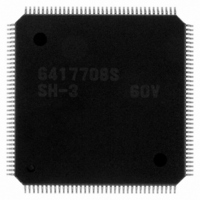
HD6417708SF60V Renesas Electronics America, HD6417708SF60V Datasheet - Page 195

HD6417708SF60V
Manufacturer Part Number
HD6417708SF60V
Description
IC SUPERH MPU ROMLESS 208LQFP
Manufacturer
Renesas Electronics America
Series
SuperH® SH7700r
Datasheet
1.HD6417708SF60V.pdf
(635 pages)
Specifications of HD6417708SF60V
Core Processor
SH-2
Core Size
32-Bit
Speed
60MHz
Connectivity
EBI/EMI, SCI, SmartCard
Peripherals
POR, WDT
Number Of I /o
8
Program Memory Type
ROMless
Voltage - Supply (vcc/vdd)
3 V ~ 3.6 V
Oscillator Type
External
Operating Temperature
-20°C ~ 75°C
Package / Case
208-LQFP
Lead Free Status / RoHS Status
Lead free / RoHS Compliant
Eeprom Size
-
Ram Size
-
Program Memory Size
-
Data Converters
-
Available stocks
Company
Part Number
Manufacturer
Quantity
Price
Company:
Part Number:
HD6417708SF60V
Manufacturer:
Renesas Electronics America
Quantity:
10 000
Part Number:
HD6417708SF60V
Manufacturer:
RENESAS/瑞萨
Quantity:
20 000
- Current page: 195 of 635
- Download datasheet (3Mb)
9.6
9.6.1
When operating in clock modes 3 and 4, the internal clock can be controlled by turning the PLL1
circuit on and off. A long oscillation settling time is required, however, when the PLL circuit is
started up from a complete halt. During this time, processor operation halts. To enable fast on/off
switching of the PLL1 circuit, the PLL standby function is provided. This function is controlled by
software using the frequency control register. The use of the PLL standby function is described
below.
9.6.2
From Off to On:
1. Initially, PSTBY = 0, PLLEN = 0, and PLL circuit 1 is stopped. The output of PLL circuit 2 is
2. When the multiplication rate of PLL circuit 1 is set in the STC1–STC0 bits and PSTBY is set
3. After PLL circuit 1 oscillation has stabilized, the input of divider 1 switches when PLLEN is
From On to Off:
1. When PLLEN is set to 0, the input of divider 1 switches to the output of PLL circuit 2. At this
2. When PSTBY is set to 0, PLL circuit 1 stops. This setting can be performed simultaneously
Notes: 1. There are some restrictions on the PLL standby state (PSTBY = 1, PLLEN = 0) as
used for divider 1 input.
to 1, PLL circuit 1 begins oscillating at the specified multiplication rate. The input to divider 1
is still the output of PLL circuit 2 at this point.
set to 1 and the oscillation output of PLL circuit 1 is divided and becomes the internal clock.
At this time, the division ratio can be changed by changing the settings of IFC1–IFC0 and
PFC1–PFC0. For several cycles before and after the clock switches, the internal clock will be
stopped, but the peripheral clock and CKIO output do not stop.
time, the division ratio can be changed by changing the settings of IFC1–IFC0 and PFC1–
PFC0.
(and with the same instruction as) the setting in 1 above.
2. It is the responsibility of software to ensure the oscillation settling time. If PLLEN is
PLL Standby Function
Overview of the PLL Standby Function
Usage
follows: The settings of the frequency control register’s CKOEN, STC2–STC0,
IFC2–IFC0 and PFC2–PFC0 bits generally cannot be changed. In some cases,
however, they can be changed if the PSTBY and PLLEN bit settings are also changed
simultaneously (figure 9.3). The SLEEP instruction cannot be executed.
set to 1 before the oscillation has settled, malfunctions may be caused by an unstable
clock.
175
Related parts for HD6417708SF60V
Image
Part Number
Description
Manufacturer
Datasheet
Request
R

Part Number:
Description:
KIT STARTER FOR M16C/29
Manufacturer:
Renesas Electronics America
Datasheet:

Part Number:
Description:
KIT STARTER FOR R8C/2D
Manufacturer:
Renesas Electronics America
Datasheet:

Part Number:
Description:
R0K33062P STARTER KIT
Manufacturer:
Renesas Electronics America
Datasheet:

Part Number:
Description:
KIT STARTER FOR R8C/23 E8A
Manufacturer:
Renesas Electronics America
Datasheet:

Part Number:
Description:
KIT STARTER FOR R8C/25
Manufacturer:
Renesas Electronics America
Datasheet:

Part Number:
Description:
KIT STARTER H8S2456 SHARPE DSPLY
Manufacturer:
Renesas Electronics America
Datasheet:

Part Number:
Description:
KIT STARTER FOR R8C38C
Manufacturer:
Renesas Electronics America
Datasheet:

Part Number:
Description:
KIT STARTER FOR R8C35C
Manufacturer:
Renesas Electronics America
Datasheet:

Part Number:
Description:
KIT STARTER FOR R8CL3AC+LCD APPS
Manufacturer:
Renesas Electronics America
Datasheet:

Part Number:
Description:
KIT STARTER FOR RX610
Manufacturer:
Renesas Electronics America
Datasheet:

Part Number:
Description:
KIT STARTER FOR R32C/118
Manufacturer:
Renesas Electronics America
Datasheet:

Part Number:
Description:
KIT DEV RSK-R8C/26-29
Manufacturer:
Renesas Electronics America
Datasheet:

Part Number:
Description:
KIT STARTER FOR SH7124
Manufacturer:
Renesas Electronics America
Datasheet:

Part Number:
Description:
KIT STARTER FOR H8SX/1622
Manufacturer:
Renesas Electronics America
Datasheet:

Part Number:
Description:
KIT DEV FOR SH7203
Manufacturer:
Renesas Electronics America
Datasheet:


