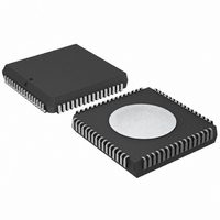
P80C592FFA/00,512 NXP Semiconductors, P80C592FFA/00,512 Datasheet - Page 44

P80C592FFA/00,512
Manufacturer Part Number
P80C592FFA/00,512
Description
IC 80C51 MCU 8BIT ROMLESS 68PLCC
Manufacturer
NXP Semiconductors
Series
80Cr
Datasheet
1.P80C592FFA00512.pdf
(108 pages)
Specifications of P80C592FFA/00,512
Program Memory Type
ROMless
Package / Case
68-PLCC
Core Processor
8051
Core Size
8-Bit
Speed
16MHz
Connectivity
CAN, EBI/EMI, UART/USART
Peripherals
DMA, POR, PWM, WDT
Number Of I /o
48
Ram Size
512 x 8
Voltage - Supply (vcc/vdd)
4.5 V ~ 5.5 V
Data Converters
A/D 8x10b
Oscillator Type
Internal
Operating Temperature
-40°C ~ 85°C
Processor Series
P80C5x
Core
80C51
Data Bus Width
8 bit
Data Ram Size
512 B
Interface Type
CAN/UART
Maximum Clock Frequency
16 MHz
Number Of Programmable I/os
40
Number Of Timers
3
Maximum Operating Temperature
+ 85 C
Mounting Style
SMD/SMT
3rd Party Development Tools
PK51, CA51, A51, ULINK2
Minimum Operating Temperature
- 40 C
On-chip Adc
8-ch x 10-bit
Cpu Family
80C
Device Core
80C51
Device Core Size
8b
Frequency (max)
16MHz
Program Memory Size
Not Required
Total Internal Ram Size
512Byte
# I/os (max)
40
Number Of Timers - General Purpose
3
Operating Supply Voltage (typ)
5V
Operating Supply Voltage (max)
5.5V
Operating Supply Voltage (min)
4.5V
Instruction Set Architecture
CISC
Operating Temp Range
-40C to 85C
Operating Temperature Classification
Industrial
Mounting
Surface Mount
Pin Count
68
Package Type
PLCC
Lead Free Status / RoHS Status
Lead free / RoHS Compliant
Eeprom Size
-
Program Memory Size
-
Lead Free Status / Rohs Status
Compliant
Other names
568-1241-5
935086530512
P80C592FFAA
935086530512
P80C592FFAA
Available stocks
Company
Part Number
Manufacturer
Quantity
Price
Company:
Part Number:
P80C592FFA/00,512
Manufacturer:
ON
Quantity:
300
Company:
Part Number:
P80C592FFA/00,512
Manufacturer:
NXP Semiconductors
Quantity:
10 000
Philips Semiconductors
13.5.11 O
The Output Control Register allows, under software
control, the set-up of different output driver configurations.
This register can be accessed (read/write) if the Reset
Request bit is set HIGH (present). If the CAN-controller is
in the sleep mode (Sleep = HIGH) a recessive level is
output on the CTX0 and CTX1 pins. If the CAN-controller
Table 49 Output Control Register (address 8)
Table 50 Description of the OCR bits
Table 51 Description of the Output Mode bits
1996 Jun 27
OCMODE1 OCMODE0
8-bit microcontroller with on-chip CAN
OCTP1
BIT
7
6
5
4
3
2
1
0
1
1
0
0
7
UTPUT
OCTP1
OCTN1
OCPOL1
OCTP0
OCTN0
OCPOL0
OCMODE1 Output Mode.
OCMODE0
SYMBOL
OCTN1
C
ONTROL
0
1
0
1
6
R
See Tables 51 and 52.
These bits select the output mode; see Table 51.
Normal Output Mode. The bit sequence (TXD) is sent via CTX0, CTX1. TXD is the data
bit to be transmitted. The voltage levels on the output driver pins CTX0 and CTX1 depend
on both the driver characteristic programmed by OCTPx, OCTNx (float, pull-up, pull-down,
push-pull) and the output polarity programmed by OCPOLx (see Fig.17).
Clock Output Mode. For the CTX0 pin this is the same as in Normal Output Mode
(CTX0: bit sequence). However, the data stream to CTX1 is replaced by the transmit clock
(TXCLK). The rising edge of the transmit clock (non-inverted) marks the beginning of a bit
period. The clock pulse width is t
Bi-phase Output Mode. In contrast to Normal Output Mode the bit representation is time
variant and toggled. If the bus controllers are galvanically decoupled from the bus-line by a
transformer, the bit stream is not allowed to contain a DC component. This is achieved by
the following scheme. During recessive bits all outputs are deactivated (floating). Dominant
bits are sent alternately on CTX0 and CTX1, i.e. the first dominant bit is sent on CTX0, the
second is sent on CTX1, and the third one is sent on CTX0 again, etc.
Test Output Mode. For the CTX0 pin this is the same as in Normal Output Mode
(CTX0: bit sequence). To measure the delay time of the transmitter and receiver this mode
connects the output of the input comparator (COMP OUT) with the input of the output driver
CTX1. This mode is used for production testing only.
EGISTER
OCPOL1
5
(OCR)
OCTP0
4
44
SCL
is in the reset state (Reset Request = HIGH) the output
drivers are floating.
Tables 50 and 51, show the relationship between the bits
of the Output Control Register and the two serial output
pins CTX0 and CTX1 of the P8xC592 CAN-controller,
connected to the serial bus (see Fig.14).
OCTN0
.
3
DESCRIPTION
FUNCTION
OCPOL0
2
OCMODE1
1
Product specification
P8xC592
OCMODE0
0


