MC908QY4ACDWE Freescale Semiconductor, MC908QY4ACDWE Datasheet - Page 20
MC908QY4ACDWE
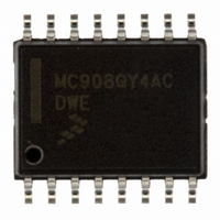
Manufacturer Part Number
MC908QY4ACDWE
Description
IC MCU 8BIT 4K FLASH 16-SOIC
Manufacturer
Freescale Semiconductor
Series
HC08r
Datasheet
1.MC908QT1ACDWE.pdf
(200 pages)
Specifications of MC908QY4ACDWE
Core Processor
HC08
Core Size
8-Bit
Speed
8MHz
Peripherals
LVD, POR, PWM
Number Of I /o
13
Program Memory Size
4KB (4K x 8)
Program Memory Type
FLASH
Ram Size
128 x 8
Voltage - Supply (vcc/vdd)
2.7 V ~ 5.5 V
Data Converters
A/D 6x10b
Oscillator Type
Internal
Operating Temperature
-40°C ~ 85°C
Package / Case
16-SOIC (0.300", 7.5mm Width)
Processor Series
HC08QY
Core
HC08
Data Bus Width
8 bit
Data Ram Size
128 B
Maximum Clock Frequency
8 MHz
Number Of Programmable I/os
13
Number Of Timers
2
Maximum Operating Temperature
+ 85 C
Mounting Style
SMD/SMT
Development Tools By Supplier
FSICEBASE, M68CBL05AE, DEMO908QB8, DEMO908QC16
Minimum Operating Temperature
- 40 C
On-chip Adc
10 bit, 6 Channel
Lead Free Status / RoHS Status
Lead free / RoHS Compliant
Eeprom Size
-
Connectivity
-
Lead Free Status / Rohs Status
Details
Available stocks
Company
Part Number
Manufacturer
Quantity
Price

Part Number:
MC908QY4ACDWE
Manufacturer:
FREESCALE
Quantity:
20 000
Part Number:
MC908QY4ACDWER
Manufacturer:
FREESCALE
Quantity:
20 000


General Description
1.6 Pin Function Priority
Table 1-3
1.7 Unused Pin Termination
Input pins and I/O port pins that are not used in the application must be terminated. This prevents excess
current caused by floating inputs, and enhances immunity during noise or transient events. Termination
methods include:
Never connect unused pins directly to V
Since some general-purpose I/O pins are not available on all packages, these pins must be terminated
as well. Either method 1 or 2 above are appropriate.
20
1. Configuring unused pins as outputs and driving high or low;
2. Configuring unused pins as inputs and enabling internal pull-ups;
3. Configuring unused pins as inputs and using external pull-up or pull-down resistors.
is meant to resolve the priority if multiple functions are enabled on a single pin.
Upon reset all pins come up as input ports regardless of the priority table.
1. When a pin is to be used as an ADC pin, the I/O port function should be left as
an input and all other shared modules should be disabled. The ADC does not
override additional modules using the pin.
Pin Name
PTB0
PTB1
PTA0
PTA1
PTA4
PTA5
PTA2
PTA3
(1)
(1)
(1)
(1)
(1)
(1)
Table 1-3. Function Priority in Shared Pins
MC68HC908QYA/QTA Family Data Sheet, Rev. 3
AD0 → TCH0 → KBI0 → PTA0
AD1 → TCH1 → KBI1 → PTA1
IRQ → TCLK → KBI2 → PTA2
RST → KBI3 → PTA3
OSC2 → AD2 → KBI4 → PTA4
OSC1 → AD3 → KBI5 → PTA5
AD4 → PTB0
AD5 → PTB1
DD
or V
Highest-to-Lowest Priority Sequence
SS
NOTE
.
Freescale Semiconductor
Related parts for MC908QY4ACDWE
Image
Part Number
Description
Manufacturer
Datasheet
Request
R

Part Number:
Description:
Manufacturer:
Freescale Semiconductor, Inc
Datasheet:
Part Number:
Description:
Manufacturer:
Freescale Semiconductor, Inc
Datasheet:
Part Number:
Description:
Manufacturer:
Freescale Semiconductor, Inc
Datasheet:
Part Number:
Description:
Manufacturer:
Freescale Semiconductor, Inc
Datasheet:
Part Number:
Description:
Manufacturer:
Freescale Semiconductor, Inc
Datasheet:
Part Number:
Description:
Manufacturer:
Freescale Semiconductor, Inc
Datasheet:
Part Number:
Description:
Manufacturer:
Freescale Semiconductor, Inc
Datasheet:
Part Number:
Description:
Manufacturer:
Freescale Semiconductor, Inc
Datasheet:
Part Number:
Description:
Manufacturer:
Freescale Semiconductor, Inc
Datasheet:
Part Number:
Description:
Manufacturer:
Freescale Semiconductor, Inc
Datasheet:
Part Number:
Description:
Manufacturer:
Freescale Semiconductor, Inc
Datasheet:
Part Number:
Description:
Manufacturer:
Freescale Semiconductor, Inc
Datasheet:
Part Number:
Description:
Manufacturer:
Freescale Semiconductor, Inc
Datasheet:
Part Number:
Description:
Manufacturer:
Freescale Semiconductor, Inc
Datasheet:
Part Number:
Description:
Manufacturer:
Freescale Semiconductor, Inc
Datasheet: