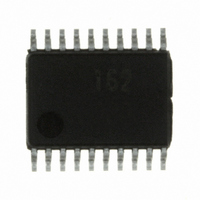
R5F21162SP#U0 Renesas Electronics America, R5F21162SP#U0 Datasheet - Page 153

R5F21162SP#U0
Manufacturer Part Number
R5F21162SP#U0
Description
IC R8C MCU FLASH 8K 20SSOP
Manufacturer
Renesas Electronics America
Series
M16C™ M16C/R8C/Tiny/16r
Datasheets
1.R5F211A2SPU0.pdf
(300 pages)
2.R5F21173DSPU0.pdf
(40 pages)
3.R5F21173DSPU0.pdf
(281 pages)
Specifications of R5F21162SP#U0
Core Processor
R8C
Core Size
16-Bit
Speed
20MHz
Connectivity
I²C, SIO, UART/USART
Peripherals
LED, POR, Voltage Detect, WDT
Number Of I /o
13
Program Memory Size
8KB (8K x 8)
Program Memory Type
FLASH
Ram Size
512 x 8
Voltage - Supply (vcc/vdd)
2.7 V ~ 5.5 V
Data Converters
A/D 4x10b
Oscillator Type
Internal
Operating Temperature
-20°C ~ 85°C
Package / Case
20-SSOP
For Use With
R0K521134S000BE - KIT EVAL STARTER FOR R8C/13
Lead Free Status / RoHS Status
Lead free / RoHS Compliant
Eeprom Size
-
- Current page: 153 of 281
- Download datasheet (4Mb)
R8C/16 Group, R8C/17 Group
Rev.2.10
REJ09B0169-0210
Figure 14.10
14.2.1
• Receive Timing When Transfer Data is 8-Bit Long (parity disabled, 1 stop bit)
Output U0BRG
RE Bit in
U0C1 Register
RXD0
Transfer Clock
RI Bit in
U0C1 Register
RI Bit in
S0RIC Register
The CNTRSEL bit in the UCON register selects whether P1_7 can be used as the CNTR00/INT10
input pin or P1_5 can be used as the CNTR01/INT11 input pin.
When the CNTRSEL bit is set to “0”, P1_7 is used as the CNTR00/INT10 pin and when the
CNTRSEL bit is set to “1”, P1_5 is used as the CNTR01/INT11 pin.
Jan 19, 2006
CNTR0 Pin Select Function
The above timing diagram applies to the following conditions.
Receive Timing in UART Mode
• PRYE bit in U0MR register = 0 (parity disabled)
• STPS bit in U0MR register = 0 (1 stop bit)
"1"
"0"
"1"
"0"
"1"
"0"
Receive starts when transfer clock is
generated by falling edge of start bit
Page 138 of 254
Start bit
Sampled "L"
D0
Receive data taken in
Set to
"0"
when interrupt request is acknowledged, or set by program
D1
Transfer from UART0 receive
register to U0RB register
D7
Stop bit
14. Serial Interface
Related parts for R5F21162SP#U0
Image
Part Number
Description
Manufacturer
Datasheet
Request
R

Part Number:
Description:
KIT STARTER FOR M16C/29
Manufacturer:
Renesas Electronics America
Datasheet:

Part Number:
Description:
KIT STARTER FOR R8C/2D
Manufacturer:
Renesas Electronics America
Datasheet:

Part Number:
Description:
R0K33062P STARTER KIT
Manufacturer:
Renesas Electronics America
Datasheet:

Part Number:
Description:
KIT STARTER FOR R8C/23 E8A
Manufacturer:
Renesas Electronics America
Datasheet:

Part Number:
Description:
KIT STARTER FOR R8C/25
Manufacturer:
Renesas Electronics America
Datasheet:

Part Number:
Description:
KIT STARTER H8S2456 SHARPE DSPLY
Manufacturer:
Renesas Electronics America
Datasheet:

Part Number:
Description:
KIT STARTER FOR R8C38C
Manufacturer:
Renesas Electronics America
Datasheet:

Part Number:
Description:
KIT STARTER FOR R8C35C
Manufacturer:
Renesas Electronics America
Datasheet:

Part Number:
Description:
KIT STARTER FOR R8CL3AC+LCD APPS
Manufacturer:
Renesas Electronics America
Datasheet:

Part Number:
Description:
KIT STARTER FOR RX610
Manufacturer:
Renesas Electronics America
Datasheet:

Part Number:
Description:
KIT STARTER FOR R32C/118
Manufacturer:
Renesas Electronics America
Datasheet:

Part Number:
Description:
KIT DEV RSK-R8C/26-29
Manufacturer:
Renesas Electronics America
Datasheet:

Part Number:
Description:
KIT STARTER FOR SH7124
Manufacturer:
Renesas Electronics America
Datasheet:

Part Number:
Description:
KIT STARTER FOR H8SX/1622
Manufacturer:
Renesas Electronics America
Datasheet:

Part Number:
Description:
KIT DEV FOR SH7203
Manufacturer:
Renesas Electronics America
Datasheet:


