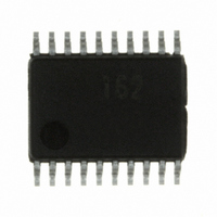
R5F21162SP#U0 Renesas Electronics America, R5F21162SP#U0 Datasheet - Page 155

R5F21162SP#U0
Manufacturer Part Number
R5F21162SP#U0
Description
IC R8C MCU FLASH 8K 20SSOP
Manufacturer
Renesas Electronics America
Series
M16C™ M16C/R8C/Tiny/16r
Datasheets
1.R5F211A2SPU0.pdf
(300 pages)
2.R5F21173DSPU0.pdf
(40 pages)
3.R5F21173DSPU0.pdf
(281 pages)
Specifications of R5F21162SP#U0
Core Processor
R8C
Core Size
16-Bit
Speed
20MHz
Connectivity
I²C, SIO, UART/USART
Peripherals
LED, POR, Voltage Detect, WDT
Number Of I /o
13
Program Memory Size
8KB (8K x 8)
Program Memory Type
FLASH
Ram Size
512 x 8
Voltage - Supply (vcc/vdd)
2.7 V ~ 5.5 V
Data Converters
A/D 4x10b
Oscillator Type
Internal
Operating Temperature
-20°C ~ 85°C
Package / Case
20-SSOP
For Use With
R0K521134S000BE - KIT EVAL STARTER FOR R8C/13
Lead Free Status / RoHS Status
Lead free / RoHS Compliant
Eeprom Size
-
- Current page: 155 of 281
- Download datasheet (4Mb)
R8C/16 Group, R8C/17 Group
Rev.2.10
REJ09B0169-0210
15. I
The I
format of the Philips I
Table 15.1 lists a Specification of IIC, Figure 15.1 shows a Block Diagram of IIC and Figure 15.2 shows the
External Circuit Connection Example of SCL and SDA Pins. Figure 15.3 to 15.8 show the registers
associated with the IIC.
* I
Table 15.1
NOTES:
Communication Format • I
I/O Pin
Transfer Clock
Receive Error Detection • Detects overrun error (clock synchronous serial format)
Interrupt Factor
Select Function
2
C bus is a trademark of Koninklijke Philips Electronics N. V.
1. The interrupt factors can use the only IIC interrupt vector table.
2
2
C bus interface (IIC) is the circuit which is used for a serial communication based on the data transfer
C bus Interface (IIC)
Jan 19, 2006
Item
Specification of IIC
2
C bus.
Page 140 of 254
• Clock Synchronous Serial Format
SCL (I/O) : Serial clock I/O pin
SDA (I/O) : Serial data I/O pin
• When the MST bit in the ICCR1 register is set to “0”
• When the MST bit in the ICCR1 register is set to “1”
• I
• Clock synchronous serial format ...... 4 types
• I
• Clock synchronous serial format
2
- Selectable for master / slave device
- Continuous transmit / receive (Since the shift register, transmit data register
- Start / stop conditions are automatically generated in master mode
- Automatic loading of acknowledge bit when transmit
- Bit synchronization / wait function (in master mode, the state of the SCL
- Direct drive of the SCL and SDA pins (NMOS open drain output) is enabled
- Continuous transmit / receive (since the shift register, transmit data register
The external clock (input from the SCL pin)
The internal clock selected by the CKS0 to CKS3 bits in the ICCR1 register
(output from the SCL pin)
An overrun error occurs during receive. When the last bit of the following data
is received while the RDRF bit in the ICSR register is set to “1” (data in the
ICDRR register), the AL bit is set to “1”.
2
Transmit data empty (including when slave address matches), transmit ends,
receive data full (including when slave address matches), arbitration lost,
NACK detection and stop condition detection.
Transmit data empty, transmit ends, receive data full and overrun error
2
- Selectable for the output level of the acknowledge signal when receive
- Selectable for the MSB-first or LSB-first to the data transfer direction
C bus format
C bus format .................................. 6 types
C bus format
and receive data register are independent)
signal is monitored per bit and the timing is synchronized automatically. If
the transfer is not possible yet, stand by to set the SCL signal to “L”.
and receive data register are independent)
Specification
(1)
(1)
15. I
2
C bus interface (IIC)
Related parts for R5F21162SP#U0
Image
Part Number
Description
Manufacturer
Datasheet
Request
R

Part Number:
Description:
KIT STARTER FOR M16C/29
Manufacturer:
Renesas Electronics America
Datasheet:

Part Number:
Description:
KIT STARTER FOR R8C/2D
Manufacturer:
Renesas Electronics America
Datasheet:

Part Number:
Description:
R0K33062P STARTER KIT
Manufacturer:
Renesas Electronics America
Datasheet:

Part Number:
Description:
KIT STARTER FOR R8C/23 E8A
Manufacturer:
Renesas Electronics America
Datasheet:

Part Number:
Description:
KIT STARTER FOR R8C/25
Manufacturer:
Renesas Electronics America
Datasheet:

Part Number:
Description:
KIT STARTER H8S2456 SHARPE DSPLY
Manufacturer:
Renesas Electronics America
Datasheet:

Part Number:
Description:
KIT STARTER FOR R8C38C
Manufacturer:
Renesas Electronics America
Datasheet:

Part Number:
Description:
KIT STARTER FOR R8C35C
Manufacturer:
Renesas Electronics America
Datasheet:

Part Number:
Description:
KIT STARTER FOR R8CL3AC+LCD APPS
Manufacturer:
Renesas Electronics America
Datasheet:

Part Number:
Description:
KIT STARTER FOR RX610
Manufacturer:
Renesas Electronics America
Datasheet:

Part Number:
Description:
KIT STARTER FOR R32C/118
Manufacturer:
Renesas Electronics America
Datasheet:

Part Number:
Description:
KIT DEV RSK-R8C/26-29
Manufacturer:
Renesas Electronics America
Datasheet:

Part Number:
Description:
KIT STARTER FOR SH7124
Manufacturer:
Renesas Electronics America
Datasheet:

Part Number:
Description:
KIT STARTER FOR H8SX/1622
Manufacturer:
Renesas Electronics America
Datasheet:

Part Number:
Description:
KIT DEV FOR SH7203
Manufacturer:
Renesas Electronics America
Datasheet:


