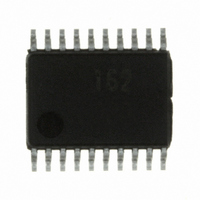
R5F21162SP#U0 Renesas Electronics America, R5F21162SP#U0 Datasheet - Page 60

R5F21162SP#U0
Manufacturer Part Number
R5F21162SP#U0
Description
IC R8C MCU FLASH 8K 20SSOP
Manufacturer
Renesas Electronics America
Series
M16C™ M16C/R8C/Tiny/16r
Datasheets
1.R5F211A2SPU0.pdf
(300 pages)
2.R5F21173DSPU0.pdf
(40 pages)
3.R5F21173DSPU0.pdf
(281 pages)
Specifications of R5F21162SP#U0
Core Processor
R8C
Core Size
16-Bit
Speed
20MHz
Connectivity
I²C, SIO, UART/USART
Peripherals
LED, POR, Voltage Detect, WDT
Number Of I /o
13
Program Memory Size
8KB (8K x 8)
Program Memory Type
FLASH
Ram Size
512 x 8
Voltage - Supply (vcc/vdd)
2.7 V ~ 5.5 V
Data Converters
A/D 4x10b
Oscillator Type
Internal
Operating Temperature
-20°C ~ 85°C
Package / Case
20-SSOP
For Use With
R0K521134S000BE - KIT EVAL STARTER FOR R8C/13
Lead Free Status / RoHS Status
Lead free / RoHS Compliant
Eeprom Size
-
- Current page: 60 of 281
- Download datasheet (4Mb)
R8C/16 Group, R8C/17 Group
Rev.2.10
REJ09B0169-0210
The following describes the clocks generated by the clock generation circuit.
9.1
Figure 9.7
This clock is supplied by a main clock oscillation circuit. This clock is used as the clock source for the
CPU and peripheral function clocks. The main clock oscillator circuit is configured by connecting a
resonator between the XIN and XOUT pins. The main clock oscillation circuit contains a feedback
resistor, which is disconnected from the oscillation circuit in stop mode in order to reduce the amount of
power consumed in the chip. The main clock oscillation circuit may also be configured by feeding an
externally generated clock to the XIN pin. Figure 9.7 shows the Examples of Main Clock Connection
Circuit.
During reset and after reset, the main clock stops.
The main clock starts oscillating when the CM05 bit in the CM0 register is set to “0” (main clock on) after
setting the CM13 bit in the CM1 register to “1” (XIN- XOUT pin).
To use the main clock for the CPU clock source, set the OCD2 bit in the OCD register to “0” (select main
clock) after the main clock is oscillating stably.
The power consumption can be reduced by setting the CM05 bit in the CM0 register to “1” (main clock
stops) if the OCD2 bit is set to “1” (select on-chip oscillator clock).
When the clocks externally generated to the XIN pin are input, a main clock does not stop if setting the
CM05 bit to “1”. If necessary, use an external circuit to stop the clock.
In stop mode, all clocks including the main clock stop. Refer to 9.4 Power Control for details.
Main Clock
Jan 19, 2006
NOTES :
Ceramic Resonator External Circuit
1. Insert a damping resistor if required. The resistance will vary depending on the oscillator and the oscillation drive
(Built-In Feedback Resistor)
XIN
capacity setting. Use the value recommended by the maker of the oscillator.
When the oscillation drive capacity is set to low, check that oscillation is stable. Also, if the oscillator manufacturer's
data sheet specifies that a feedback resistor be added external to the chip, insert a feedback resistor between XIN
and XOUT following the instruction.
Examples of Main Clock Connection Circuit
CIN
Microcomputer
Page 45 of 254
XOUT
Rd
COUT
(1)
VCC
VSS
Externally Derived Clock
(Built-In Feedback Resistor)
External Clock Input Circuit
XIN
Microcomputer
9. Clock Generation Circuit
XOUT
Open
Related parts for R5F21162SP#U0
Image
Part Number
Description
Manufacturer
Datasheet
Request
R

Part Number:
Description:
KIT STARTER FOR M16C/29
Manufacturer:
Renesas Electronics America
Datasheet:

Part Number:
Description:
KIT STARTER FOR R8C/2D
Manufacturer:
Renesas Electronics America
Datasheet:

Part Number:
Description:
R0K33062P STARTER KIT
Manufacturer:
Renesas Electronics America
Datasheet:

Part Number:
Description:
KIT STARTER FOR R8C/23 E8A
Manufacturer:
Renesas Electronics America
Datasheet:

Part Number:
Description:
KIT STARTER FOR R8C/25
Manufacturer:
Renesas Electronics America
Datasheet:

Part Number:
Description:
KIT STARTER H8S2456 SHARPE DSPLY
Manufacturer:
Renesas Electronics America
Datasheet:

Part Number:
Description:
KIT STARTER FOR R8C38C
Manufacturer:
Renesas Electronics America
Datasheet:

Part Number:
Description:
KIT STARTER FOR R8C35C
Manufacturer:
Renesas Electronics America
Datasheet:

Part Number:
Description:
KIT STARTER FOR R8CL3AC+LCD APPS
Manufacturer:
Renesas Electronics America
Datasheet:

Part Number:
Description:
KIT STARTER FOR RX610
Manufacturer:
Renesas Electronics America
Datasheet:

Part Number:
Description:
KIT STARTER FOR R32C/118
Manufacturer:
Renesas Electronics America
Datasheet:

Part Number:
Description:
KIT DEV RSK-R8C/26-29
Manufacturer:
Renesas Electronics America
Datasheet:

Part Number:
Description:
KIT STARTER FOR SH7124
Manufacturer:
Renesas Electronics America
Datasheet:

Part Number:
Description:
KIT STARTER FOR H8SX/1622
Manufacturer:
Renesas Electronics America
Datasheet:

Part Number:
Description:
KIT DEV FOR SH7203
Manufacturer:
Renesas Electronics America
Datasheet:


