M30840SGP#U5 Renesas Electronics America, M30840SGP#U5 Datasheet - Page 117
M30840SGP#U5
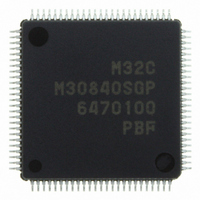
Manufacturer Part Number
M30840SGP#U5
Description
IC M32C/84 MCU ROMLESS 100LQFP
Manufacturer
Renesas Electronics America
Series
M16C™ M32C/80r
Datasheet
1.M30843FWGPU5.pdf
(531 pages)
Specifications of M30840SGP#U5
Core Processor
M32C/80
Core Size
16/32-Bit
Speed
32MHz
Connectivity
CAN, I²C, IEBus, SIO, UART/USART
Peripherals
DMA, PWM, WDT
Number Of I /o
45
Program Memory Type
ROMless
Ram Size
10K x 8
Voltage - Supply (vcc/vdd)
3 V ~ 5.5 V
Data Converters
A/D 10x10b, D/A 2x8b
Oscillator Type
Internal
Operating Temperature
-20°C ~ 85°C
Package / Case
100-LQFP
For Use With
R0K330879S001BE - KIT DEV RSK M32C/87R0K330879S000BE - KIT DEV RSK M32C/87
Lead Free Status / RoHS Status
Lead free / RoHS Compliant
Eeprom Size
-
Program Memory Size
-
Available stocks
Company
Part Number
Manufacturer
Quantity
Price

Part Number:
M30840SGP#U5M30840SGP#U3
Manufacturer:
Renesas Electronics America
Quantity:
10 000


M
R
R
e
E
3
. v
J
2
Figure 9.12 Procedure to Use PLL Clock as CPU Clock Source
Table 9.3 Bit Settings to Use PLL Clock as CPU Clock Source
0
C
9.1.4 PLL Clock
1
9
0 .
8 /
B
1
The PLL frequency synthesizer generates the PLL clock based on the main clock. The PLL clock can be
used as clock source for the CPU clock and peripheral function clock.
The PLL frequency synthesizer stops after reset. When the PLC07 bit is set to "1" (PLL on), the PLL
frequency synthesizer starts operating. Wait
The PLL clock can either be the clock output from the voltage controlled oscillator (VCO) divided-by-2 or
divided-by-3. When the PLL clock is used as a clock source for the CPU clock or peripheral function
clock, set each bit as is shown in Table 9.3. Figure 9.12 shows the procedure to use the PLL clock as the
CPU clock source.
To enter wait or stop mode, set the CM17 bit to "0" (main clock as CPU clock source), set the PLC07 bit
in the PLC0 register to "0" (PLL off) and then enter wait or stop mode.
8
f
0
0
1
4
X (
0
M
M
3
G
J
N I
H
6
u
H
o r
)
z
0 -
. l
z
u
0
1
p
, 7
0
1
(
2
M
P
0
3
L
0
C
2
5
C
0
0
1
2
8 /
Page 94
B
, 4
t i
M
P
3
L
P
2
Use PLL clock as CPU clock source
C
L
C
Set the PLC0 and the PLC1 registers
0
(PLL clock as CPU clock source)
C
f o
8 /
R
0
0
1
4
e
1
4
Set the PLC07 bit to "1"
(Set the PLC07 bit to "0")
) T
g
Set the CM17 bit to "1"
9
B
t s i
5
t i
r e
Wait tsu
(PLL on)
P
L
End
C
(PLL)
0
0
1
0
B
ms
t i
tsu
(PLL)
P
L
C
C
M
1
ms for the PLL clock to stabilize.
2
R
0
0
1
1
1
e
g
B
t s i
t i
r e
PLC07 bit : Bit in the PLC0 Register
CM17 bit : Bit in the CM1 Register
P
2
3
3
2
L
1
0
0
2
L
3 .
M
M
M
C
M
H
H
H
o l
H
z
z
z
k c
z
9. Clock Generation Circuit
Related parts for M30840SGP#U5
Image
Part Number
Description
Manufacturer
Datasheet
Request
R

Part Number:
Description:
KIT STARTER FOR M16C/29
Manufacturer:
Renesas Electronics America
Datasheet:

Part Number:
Description:
KIT STARTER FOR R8C/2D
Manufacturer:
Renesas Electronics America
Datasheet:

Part Number:
Description:
R0K33062P STARTER KIT
Manufacturer:
Renesas Electronics America
Datasheet:

Part Number:
Description:
KIT STARTER FOR R8C/23 E8A
Manufacturer:
Renesas Electronics America
Datasheet:

Part Number:
Description:
KIT STARTER FOR R8C/25
Manufacturer:
Renesas Electronics America
Datasheet:

Part Number:
Description:
KIT STARTER H8S2456 SHARPE DSPLY
Manufacturer:
Renesas Electronics America
Datasheet:

Part Number:
Description:
KIT STARTER FOR R8C38C
Manufacturer:
Renesas Electronics America
Datasheet:

Part Number:
Description:
KIT STARTER FOR R8C35C
Manufacturer:
Renesas Electronics America
Datasheet:

Part Number:
Description:
KIT STARTER FOR R8CL3AC+LCD APPS
Manufacturer:
Renesas Electronics America
Datasheet:
Part Number:
Description:
KIT STARTER FOR RX610
Manufacturer:
Renesas Electronics America
Datasheet:

Part Number:
Description:
KIT STARTER FOR R32C/118
Manufacturer:
Renesas Electronics America
Datasheet:

Part Number:
Description:
KIT DEV RSK-R8C/26-29
Manufacturer:
Renesas Electronics America
Datasheet:

Part Number:
Description:
KIT STARTER FOR SH7124
Manufacturer:
Renesas Electronics America
Datasheet:

Part Number:
Description:
KIT STARTER FOR H8SX/1622
Manufacturer:
Renesas Electronics America
Datasheet:

Part Number:
Description:
KIT DEV FOR SH7203
Manufacturer:
Renesas Electronics America
Datasheet: