M30840SGP#U5 Renesas Electronics America, M30840SGP#U5 Datasheet - Page 417
M30840SGP#U5
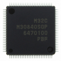
Manufacturer Part Number
M30840SGP#U5
Description
IC M32C/84 MCU ROMLESS 100LQFP
Manufacturer
Renesas Electronics America
Series
M16C™ M32C/80r
Datasheet
1.M30843FWGPU5.pdf
(531 pages)
Specifications of M30840SGP#U5
Core Processor
M32C/80
Core Size
16/32-Bit
Speed
32MHz
Connectivity
CAN, I²C, IEBus, SIO, UART/USART
Peripherals
DMA, PWM, WDT
Number Of I /o
45
Program Memory Type
ROMless
Ram Size
10K x 8
Voltage - Supply (vcc/vdd)
3 V ~ 5.5 V
Data Converters
A/D 10x10b, D/A 2x8b
Oscillator Type
Internal
Operating Temperature
-20°C ~ 85°C
Package / Case
100-LQFP
For Use With
R0K330879S001BE - KIT DEV RSK M32C/87R0K330879S000BE - KIT DEV RSK M32C/87
Lead Free Status / RoHS Status
Lead free / RoHS Compliant
Eeprom Size
-
Program Memory Size
-
Available stocks
Company
Part Number
Manufacturer
Quantity
Price

Part Number:
M30840SGP#U5M30840SGP#U3
Manufacturer:
Renesas Electronics America
Quantity:
10 000


M
R
R
e
E
3
. v
J
2
Table 24.5 Port P8 Peripheral Function Output Control
Table 24.6 Port P9 Peripheral Function Output Control
Table 24.7 Port P10 Peripheral Function Input Control
0
Bit 0
Bit 1
Bit 2
Bit 3 to 7 Set to "00000
Bit 0 0: P9
Bit 1 0: P9
Bit 2 0: P9
Bit 3
Bit 4
Bit 5 0: P9
Bit 6 0: P9
Bit 7
Bit 7
C
1
9
0 .
8 /
B
0
1
4
0
PS3 Register
1: CLK3(output)
1: Selected by the PSL3 register
1: Selected by the PSL3 register
0: P9
1: RTS3
0: P9
1: RTS4
1: CLK4(output)
1: Selected by the PSC3 register
0: P9
1: Selected by the PSL3 register
PSC Register
0: P10
1: AN
3
G
J
6
u
o r
0 -
. l
________
________
u
0: P8
0: P8
1: Selected by the PSL2 register
0: P8
1: Selected by the PSL2 register
0
1
1: Selected by the PSL2 register
0
1
2
3
4
5
6
7
p
PS2 Register
4
, 7
0
/TB0
/TB1
/TB2
/TB3
/TB4
/ANEX0/CLK4(input)
/SRxD4/ANEX1/SDA4(input)
/RxD
4
1
to AN
(
to P10
2
M
0
0
1
2
3
/ISRxD0/TA4
/INT0
0
/TA4
IN
IN
IN
IN
IN
________
4
2
5
/AD
/CLK3(input)
/RxD3/SCL3(input)
/SRxD3/SDA3(input)
/CTS3/SS3/DA0(output)
/CTS4/SS4/DA1(output)
7
C
__________
_______
________
7
8 /
IN
Page 394
TRG
or KI0 to KI3
, 4
/INPC1
2
_____
"
_______
/SCL4(input)
M
______
3
2
OUT
5
C
_____
f o
8 /
(input)
4
4
) T
9
5
PSL2 Register
0: TA4
1: U
0: U
1: Selected by the PSC2 register
0: Do not set to this value
1: Selected by the PSC2 register
PSL3 Register
Set to "0"
0: SCL3(output)
1: STxD3
0: TxD3/SDA3(output)
1: Do not set to this value
0: Except DA0
1: DA0
0: Except DA1
1: DA1
0: Except ANEX0
1: ANEX0
0: Except ANEX1
1: ANEX1
0: SCL4(output
1: STxD4
____
OUT
(output)
)
PSC3 Register
Set to "0"
Set to "0"
Set to "0"
Set to "0"
Set to "0"
Set to "0"
0: TxD4/SDA4
1: Do not set to this value
Set to "0"
PSC2 Register
Set to "0"
0: Do not set to this value
1: OUTC1
0: CAN0
1: Do not set to this value
24. Programmable I/O Ports
OUT
5
Related parts for M30840SGP#U5
Image
Part Number
Description
Manufacturer
Datasheet
Request
R

Part Number:
Description:
KIT STARTER FOR M16C/29
Manufacturer:
Renesas Electronics America
Datasheet:

Part Number:
Description:
KIT STARTER FOR R8C/2D
Manufacturer:
Renesas Electronics America
Datasheet:

Part Number:
Description:
R0K33062P STARTER KIT
Manufacturer:
Renesas Electronics America
Datasheet:

Part Number:
Description:
KIT STARTER FOR R8C/23 E8A
Manufacturer:
Renesas Electronics America
Datasheet:

Part Number:
Description:
KIT STARTER FOR R8C/25
Manufacturer:
Renesas Electronics America
Datasheet:

Part Number:
Description:
KIT STARTER H8S2456 SHARPE DSPLY
Manufacturer:
Renesas Electronics America
Datasheet:

Part Number:
Description:
KIT STARTER FOR R8C38C
Manufacturer:
Renesas Electronics America
Datasheet:

Part Number:
Description:
KIT STARTER FOR R8C35C
Manufacturer:
Renesas Electronics America
Datasheet:

Part Number:
Description:
KIT STARTER FOR R8CL3AC+LCD APPS
Manufacturer:
Renesas Electronics America
Datasheet:
Part Number:
Description:
KIT STARTER FOR RX610
Manufacturer:
Renesas Electronics America
Datasheet:

Part Number:
Description:
KIT STARTER FOR R32C/118
Manufacturer:
Renesas Electronics America
Datasheet:

Part Number:
Description:
KIT DEV RSK-R8C/26-29
Manufacturer:
Renesas Electronics America
Datasheet:

Part Number:
Description:
KIT STARTER FOR SH7124
Manufacturer:
Renesas Electronics America
Datasheet:

Part Number:
Description:
KIT STARTER FOR H8SX/1622
Manufacturer:
Renesas Electronics America
Datasheet:

Part Number:
Description:
KIT DEV FOR SH7203
Manufacturer:
Renesas Electronics America
Datasheet: