M30840SGP#U5 Renesas Electronics America, M30840SGP#U5 Datasheet - Page 521
M30840SGP#U5
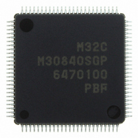
Manufacturer Part Number
M30840SGP#U5
Description
IC M32C/84 MCU ROMLESS 100LQFP
Manufacturer
Renesas Electronics America
Series
M16C™ M32C/80r
Datasheet
1.M30843FWGPU5.pdf
(531 pages)
Specifications of M30840SGP#U5
Core Processor
M32C/80
Core Size
16/32-Bit
Speed
32MHz
Connectivity
CAN, I²C, IEBus, SIO, UART/USART
Peripherals
DMA, PWM, WDT
Number Of I /o
45
Program Memory Type
ROMless
Ram Size
10K x 8
Voltage - Supply (vcc/vdd)
3 V ~ 5.5 V
Data Converters
A/D 10x10b, D/A 2x8b
Oscillator Type
Internal
Operating Temperature
-20°C ~ 85°C
Package / Case
100-LQFP
For Use With
R0K330879S001BE - KIT DEV RSK M32C/87R0K330879S000BE - KIT DEV RSK M32C/87
Lead Free Status / RoHS Status
Lead free / RoHS Compliant
Eeprom Size
-
Program Memory Size
-
Available stocks
Company
Part Number
Manufacturer
Quantity
Price

Part Number:
M30840SGP#U5M30840SGP#U3
Manufacturer:
Renesas Electronics America
Quantity:
10 000


Rev.
REVISION HISTORY
Date
77-80
Page
48
49
50
51
52
52
52
53
54
55
57
58
59
60
66
67
82
84
86
87
89
92
95
96
-
Voltage Detection Circuit
New Chapter
• 6. Voltage Detection Circuit Note added; Description modified
• Figure 6.1 Reset Circuit Block Diagram modified
• Figure 6.2 WDC Register and VCR1 Register Note 3 added to the WDC regis-
• Figure 6.3 VCR2 Register Note 2 deleted; notes 5 and 6 added
• Figure 6.4 D4INT Register Note 6 added
• 6.1 Voltage Down Detection Interrupt Description modified
• Table 6.1 Conditions to Generate the Voltage Down Detect interrupt Request
• Table 6.2 Sampling Periods Table modified
• Figure 6.5 Voltage Down Detection interrupt Generating Circuit Compo-
• 6.2 Cold Start-up / Warm Start-up Determine Function Newly added
Processor Mode
• Chapter structuer modified
• Figure 7.1 PM0 Register Notes 2 and 8 added
• Figure 7.2 PM1 Register Note 3 added
• Figure 7.3 Memory Map in Each Processor Mode Figure partially modified;
Bus
• 8. Bus Note added
• Figure 8.1 DS Register Note 1 modified
• Figure 8.3 EWCR0 to EWCR3 Registers Note 3 added
• Table 8.5 Software Wait State and Bus Cycle Value of the EWCRi04 to
• 8.3 Page Mode Control Function Added
Clock Generation Circuit
• Figure 9.1 Clock Generation Circuit Block diagram modified; f
• Figure 9.3 CM1 Register Note mark position changed
• Figure 9.5 CM2 Register Note 2 added to TCSPR, COSRF and TCSPR regis-
• Figure 9.6 TCSPR and CPSRF Registers Note 2 added to the TCSPR register
• Figure 9.8 PM2 Register The PM24 and PM25 bits newly available
• Table 9.2 Bit Settings for On-Chip Oscillator Start Condition Newly added
• Table 9.4 CPU Clock Source and Bit Settings Main clock (main clock direct
• 9.3.4 f
ter; note 1 deleted from and note 2 added to the VCR1 register
D42 bit setting modified
nent name modified
Note 3 added
EWCRi00 bits revised
ters
mode), the PM24 bit in the PM2 register and note 1 added
CAN
M32C/84 Group(M32C/84, M32C/84T) Hardware Manual
Newly added
C-3
Description
Summary
CAN
added
Related parts for M30840SGP#U5
Image
Part Number
Description
Manufacturer
Datasheet
Request
R

Part Number:
Description:
KIT STARTER FOR M16C/29
Manufacturer:
Renesas Electronics America
Datasheet:

Part Number:
Description:
KIT STARTER FOR R8C/2D
Manufacturer:
Renesas Electronics America
Datasheet:

Part Number:
Description:
R0K33062P STARTER KIT
Manufacturer:
Renesas Electronics America
Datasheet:

Part Number:
Description:
KIT STARTER FOR R8C/23 E8A
Manufacturer:
Renesas Electronics America
Datasheet:

Part Number:
Description:
KIT STARTER FOR R8C/25
Manufacturer:
Renesas Electronics America
Datasheet:

Part Number:
Description:
KIT STARTER H8S2456 SHARPE DSPLY
Manufacturer:
Renesas Electronics America
Datasheet:

Part Number:
Description:
KIT STARTER FOR R8C38C
Manufacturer:
Renesas Electronics America
Datasheet:

Part Number:
Description:
KIT STARTER FOR R8C35C
Manufacturer:
Renesas Electronics America
Datasheet:

Part Number:
Description:
KIT STARTER FOR R8CL3AC+LCD APPS
Manufacturer:
Renesas Electronics America
Datasheet:
Part Number:
Description:
KIT STARTER FOR RX610
Manufacturer:
Renesas Electronics America
Datasheet:

Part Number:
Description:
KIT STARTER FOR R32C/118
Manufacturer:
Renesas Electronics America
Datasheet:

Part Number:
Description:
KIT DEV RSK-R8C/26-29
Manufacturer:
Renesas Electronics America
Datasheet:

Part Number:
Description:
KIT STARTER FOR SH7124
Manufacturer:
Renesas Electronics America
Datasheet:

Part Number:
Description:
KIT STARTER FOR H8SX/1622
Manufacturer:
Renesas Electronics America
Datasheet:

Part Number:
Description:
KIT DEV FOR SH7203
Manufacturer:
Renesas Electronics America
Datasheet: