M30840SGP#U5 Renesas Electronics America, M30840SGP#U5 Datasheet - Page 519
M30840SGP#U5
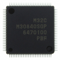
Manufacturer Part Number
M30840SGP#U5
Description
IC M32C/84 MCU ROMLESS 100LQFP
Manufacturer
Renesas Electronics America
Series
M16C™ M32C/80r
Datasheet
1.M30843FWGPU5.pdf
(531 pages)
Specifications of M30840SGP#U5
Core Processor
M32C/80
Core Size
16/32-Bit
Speed
32MHz
Connectivity
CAN, I²C, IEBus, SIO, UART/USART
Peripherals
DMA, PWM, WDT
Number Of I /o
45
Program Memory Type
ROMless
Ram Size
10K x 8
Voltage - Supply (vcc/vdd)
3 V ~ 5.5 V
Data Converters
A/D 10x10b, D/A 2x8b
Oscillator Type
Internal
Operating Temperature
-20°C ~ 85°C
Package / Case
100-LQFP
For Use With
R0K330879S001BE - KIT DEV RSK M32C/87R0K330879S000BE - KIT DEV RSK M32C/87
Lead Free Status / RoHS Status
Lead free / RoHS Compliant
Eeprom Size
-
Program Memory Size
-
Available stocks
Company
Part Number
Manufacturer
Quantity
Price

Part Number:
M30840SGP#U5M30840SGP#U3
Manufacturer:
Renesas Electronics America
Quantity:
10 000


1.00
0.41
0.50
Rev.
Apr., 05
Mar., 03
Jun., 04
REVISION HISTORY
Date
All pages
Page
128
129
186
387
388
390
391
392
393
413
415
416
418
425
429
430
436
1
-
-
New Document
Words standardized: On-chip oscillator, A/D converter and D/A converter
Interrupts
• Figure 10.15 IIO0IE to IIO5IE, IIO8IE to IIO11IE Registers Note 2 added
Watchdog Timer
• Figure 11.1 Watchdog Timer Block Diagram modified
Three-Phase Motor Control Timer Functions
• Figure 15.5 ICTB Register, TA1, TA2, TA4, TA11, TA21 and TA41 Registers and
Flash Memory Version
• Figure 24.4 FMR0 Register Notes 1 and 7 revised
• Figure 24.5 FMR1 Register Notes 1 revised
• Figure 24.6 How to Enter and Exit EW0 Mode Note 2 revised; note 5 added
• Figure 24.7 How to Enter and Exit EW1 Mode Note 3 revised; note 4 added
• Figure 24.8 Handling Before and After Low Power Consumption Mode
• 24.3.4.5 How to Access Description modified
Electrical Characteristics
• Table 25.2 Recommended Operating Conditions f
• Table 25.3 Electrical Characteristics R
• Table 25.4 A/D Conversion Characteristics t
• Table 25.7 Low Voltage Detect Circuit Electrical Characteristics added
• Table 25.8 Power Supply Timing added
• Figure 25.1 Power Supply Timing Diagram added
• Figure 25.3 V
• Table 25.24 Electrical Characteristics R
• Table 25.25 A/D Conversion Characteristics t
• Figure 25.7 V
Precautions
• Section of Three-Phase Control Timer Functions delected
M32C/84T (High-reliability version) added
Description for the reserved bits on register diagrams modified
Overview
• 1.1 Applications Automobiles added
TB2SC Register Note 7 for TA1, TA2, TA4, TA11, TA21 and TA41 registers deleted
Notes 4 and 5 added
SV
version added
sion modified
version added
sion modified
CC
and note 1 deleted
M32C/84 Group(M32C/84, M32C/84T) Hardware Manual
CC1
CC1
=V
=V
CC2
CC2
C-1
=5V Timing Diagram (1) tac1
=5V Timing Diagram (1) tac1
Description
Summary
PULLUP
PULLUP
SMP
CONV
value modified; note 1 added
value for the masked ROM
value for the masked ROM
(AD-DB)
(AD-DB)
value modified
(ripple)
, Vp-p
arithmetic expres-
arithmetic expres-
(ripple)
, V
CC
,
Related parts for M30840SGP#U5
Image
Part Number
Description
Manufacturer
Datasheet
Request
R

Part Number:
Description:
KIT STARTER FOR M16C/29
Manufacturer:
Renesas Electronics America
Datasheet:

Part Number:
Description:
KIT STARTER FOR R8C/2D
Manufacturer:
Renesas Electronics America
Datasheet:

Part Number:
Description:
R0K33062P STARTER KIT
Manufacturer:
Renesas Electronics America
Datasheet:

Part Number:
Description:
KIT STARTER FOR R8C/23 E8A
Manufacturer:
Renesas Electronics America
Datasheet:

Part Number:
Description:
KIT STARTER FOR R8C/25
Manufacturer:
Renesas Electronics America
Datasheet:

Part Number:
Description:
KIT STARTER H8S2456 SHARPE DSPLY
Manufacturer:
Renesas Electronics America
Datasheet:

Part Number:
Description:
KIT STARTER FOR R8C38C
Manufacturer:
Renesas Electronics America
Datasheet:

Part Number:
Description:
KIT STARTER FOR R8C35C
Manufacturer:
Renesas Electronics America
Datasheet:

Part Number:
Description:
KIT STARTER FOR R8CL3AC+LCD APPS
Manufacturer:
Renesas Electronics America
Datasheet:
Part Number:
Description:
KIT STARTER FOR RX610
Manufacturer:
Renesas Electronics America
Datasheet:

Part Number:
Description:
KIT STARTER FOR R32C/118
Manufacturer:
Renesas Electronics America
Datasheet:

Part Number:
Description:
KIT DEV RSK-R8C/26-29
Manufacturer:
Renesas Electronics America
Datasheet:

Part Number:
Description:
KIT STARTER FOR SH7124
Manufacturer:
Renesas Electronics America
Datasheet:

Part Number:
Description:
KIT STARTER FOR H8SX/1622
Manufacturer:
Renesas Electronics America
Datasheet:

Part Number:
Description:
KIT DEV FOR SH7203
Manufacturer:
Renesas Electronics America
Datasheet: