M30840SGP#U5 Renesas Electronics America, M30840SGP#U5 Datasheet - Page 527
M30840SGP#U5
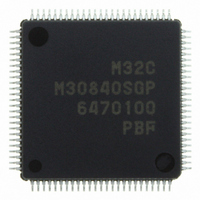
Manufacturer Part Number
M30840SGP#U5
Description
IC M32C/84 MCU ROMLESS 100LQFP
Manufacturer
Renesas Electronics America
Series
M16C™ M32C/80r
Datasheet
1.M30843FWGPU5.pdf
(531 pages)
Specifications of M30840SGP#U5
Core Processor
M32C/80
Core Size
16/32-Bit
Speed
32MHz
Connectivity
CAN, I²C, IEBus, SIO, UART/USART
Peripherals
DMA, PWM, WDT
Number Of I /o
45
Program Memory Type
ROMless
Ram Size
10K x 8
Voltage - Supply (vcc/vdd)
3 V ~ 5.5 V
Data Converters
A/D 10x10b, D/A 2x8b
Oscillator Type
Internal
Operating Temperature
-20°C ~ 85°C
Package / Case
100-LQFP
For Use With
R0K330879S001BE - KIT DEV RSK M32C/87R0K330879S000BE - KIT DEV RSK M32C/87
Lead Free Status / RoHS Status
Lead free / RoHS Compliant
Eeprom Size
-
Program Memory Size
-
Available stocks
Company
Part Number
Manufacturer
Quantity
Price

Part Number:
M30840SGP#U5M30840SGP#U3
Manufacturer:
Renesas Electronics America
Quantity:
10 000


Rev.
REVISION HISTORY
Date
Page
104
105
113
124
131
162
164
165
170
171
176
177
178
180
194
196
197
198
202
213
225
226
58
62
87
Processor Mode
• Figure 7.2 PM1 Register PM13 bit function changed
Bus
• Table 8.2 Processor Mode and Port Function Note 3 modified
Clock Generation Circuit
• Figure 9.6 TCSPR Register Value after reset modified
• Figure 9.14 Status Transition Note 4 repleaced to note 5
• 9.6 System Clock Protection Function Description modified
Interrupt
• Table 11.2 Relocatable Vector Table Fault Error deleted; Note 4 deleted
• Figure 11.10 IFSR Register IFSR6 and IFSR7 bit functions changed
Watchdog Timer
• Chapter description modified
Timer
• Table 15.3 Timer Mode Specifications Write to Timer specification changed
• Table 15.4 Event Counter Mode Specifications Write to Timer specification
• Table 15.5 Event Counter Mode Specifications Write to Timer specification
• Table 15.7 Pulse Width Modulation Mode Specifications Write to Timer
• Figure 15.13 TA0MR to TA4MR Registers Value after reset modified
• Table 15.9 Timer Mode Specifications Write to Timer specification changed
• Table 15.10 Event Counter Mode Specifications Write to Timer specification
• Figure 15.21 TB0MR to TB5MR Registers TCK1 bit name modified
• Figure 15.22 TB0MR to TB5MR Registers Notes 1 and 2 modified
Serial I/O
• Figure 17.1 UARTi Block Diagram Diagram modified
• Figure 17.3 U0MR to U4MR Registers Value after reset modified
• Figure 17.4 U0C0 to U4C0 Registers Note 1 modified
• Figure 17.5 U0C1 to U4C1 Registers Note 2 modified
• Figure 17.9 IFSR Register IFSR6 and IFSR7 bit functions changed
• Table 17.13 Register Settings in I
• 17.3.6 SDA Input The IICM bit in the description modified to the IICM2 bit
• Table 17.19 Special Mode 2 Specifications Transmit/Receive Control speci-
changed
changed
specification changed
changed
fication changed; Transmit Start Condision specification changed; Error Detec-
tion specification changed
M32C/84 Group(M32C/84, M32C/84T) Hardware Manual
C-9
Description
2
Summary
C Mode SWC and ALS bit functions modified
Related parts for M30840SGP#U5
Image
Part Number
Description
Manufacturer
Datasheet
Request
R

Part Number:
Description:
KIT STARTER FOR M16C/29
Manufacturer:
Renesas Electronics America
Datasheet:

Part Number:
Description:
KIT STARTER FOR R8C/2D
Manufacturer:
Renesas Electronics America
Datasheet:

Part Number:
Description:
R0K33062P STARTER KIT
Manufacturer:
Renesas Electronics America
Datasheet:

Part Number:
Description:
KIT STARTER FOR R8C/23 E8A
Manufacturer:
Renesas Electronics America
Datasheet:

Part Number:
Description:
KIT STARTER FOR R8C/25
Manufacturer:
Renesas Electronics America
Datasheet:

Part Number:
Description:
KIT STARTER H8S2456 SHARPE DSPLY
Manufacturer:
Renesas Electronics America
Datasheet:

Part Number:
Description:
KIT STARTER FOR R8C38C
Manufacturer:
Renesas Electronics America
Datasheet:

Part Number:
Description:
KIT STARTER FOR R8C35C
Manufacturer:
Renesas Electronics America
Datasheet:

Part Number:
Description:
KIT STARTER FOR R8CL3AC+LCD APPS
Manufacturer:
Renesas Electronics America
Datasheet:
Part Number:
Description:
KIT STARTER FOR RX610
Manufacturer:
Renesas Electronics America
Datasheet:

Part Number:
Description:
KIT STARTER FOR R32C/118
Manufacturer:
Renesas Electronics America
Datasheet:

Part Number:
Description:
KIT DEV RSK-R8C/26-29
Manufacturer:
Renesas Electronics America
Datasheet:

Part Number:
Description:
KIT STARTER FOR SH7124
Manufacturer:
Renesas Electronics America
Datasheet:

Part Number:
Description:
KIT STARTER FOR H8SX/1622
Manufacturer:
Renesas Electronics America
Datasheet:

Part Number:
Description:
KIT DEV FOR SH7203
Manufacturer:
Renesas Electronics America
Datasheet: