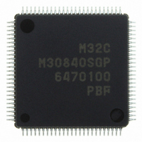
M30840SGP#U5 Renesas Electronics America, M30840SGP#U5 Datasheet - Page 464

M30840SGP#U5
Manufacturer Part Number
M30840SGP#U5
Description
IC M32C/84 MCU ROMLESS 100LQFP
Manufacturer
Renesas Electronics America
Series
M16C™ M32C/80r
Datasheet
1.M30843FWGPU5.pdf
(531 pages)
Specifications of M30840SGP#U5
Core Processor
M32C/80
Core Size
16/32-Bit
Speed
32MHz
Connectivity
CAN, I²C, IEBus, SIO, UART/USART
Peripherals
DMA, PWM, WDT
Number Of I /o
45
Program Memory Type
ROMless
Ram Size
10K x 8
Voltage - Supply (vcc/vdd)
3 V ~ 5.5 V
Data Converters
A/D 10x10b, D/A 2x8b
Oscillator Type
Internal
Operating Temperature
-20°C ~ 85°C
Package / Case
100-LQFP
For Use With
R0K330879S001BE - KIT DEV RSK M32C/87R0K330879S000BE - KIT DEV RSK M32C/87
Lead Free Status / RoHS Status
Lead free / RoHS Compliant
Eeprom Size
-
Program Memory Size
-
Available stocks
Company
Part Number
Manufacturer
Quantity
Price
Part Number:
M30840SGP#U5M30840SGP#U3
Manufacturer:
Renesas Electronics America
Quantity:
10 000
- Current page: 464 of 531
- Download datasheet (4Mb)
R
R
M
e
E
3
. v
J
Figure 26.3 V
2
0
1
C
9
0 .
B
8 /
0
1
4
0
Memory Expansion Mode and Microprocessor Mode
(when accessing an external memory space)
3
CSi
ADi
BHE
J
BCLK
CSi
ADi
BHE
WR,WRL,
WRH
DBi
RD
DB
NOTES:
BCLK
G
[ Read Timing ]
6
[ Write timing ]
u
0 -
. l
o r
NOTES:
0
1
u
A maximum of 35ns is guaranteed for t
1. Values guaranteed only when the microcomputer is used independently.
2. Varies with operation frequency:
, 7
0
p
3. Varies with operation frequency:
1
2
(
t
(if external bus cycle is a +b , m=b)
t
t
t
t
(if external bus cycle is a +b , n=(bx2)-1)
M
CC1
0
d(DB-WR)
h(WR-DB)
h(WR-AD)
h(WR-CS)
w(WR)
t
t
ac1(RD-DB)
ac1(AD-DB)
0
3
t
d(BCLK-AD)
5
2
=V
=(tcyc/2 x n-15)ns.min
C
Page 441
8 /
=(tcyc x m-20)ns.min
=(tcyc/2-10)ns.min
=(tcyc/2-10)ns.min
=(tcyc/2-10)ns.min
t
t
CC2
18ns.max
t
18ns.max
18ns.max
18ns.max
18ns.max
d(BCLK-CS)
t
d(BCLK-AD)
d(BCLK-CS)
d(BCLK-RD)
, 4
=(tcyc x n-35)ns.max (if external bus cycle is a + b , n=a+b)
=(tcyc/2 x m-35)ns.max (if external bus cycle is a + b , m=(b x 2)+1)
=5V Timing Diagram (1)
tcyc
M
(1 +1 Bus Cycle)
tcyc
(1 +1 Bus Cycle)
3
2
(1)
(1)
C
f o
8 /
t
t
d(BCLK-WR)
18ns.max
4
ac1(AD-DB)
4
9
) T
Hi-Z
5
t
d(DB-WR)
d(BCLK-AD)
(2)
t
ac1(RD-DB)
(3)
t
t
w(WR)
su(DB-BCLK)
26ns.min
+t
(3)
su(DB-BCLK)
(2)
Measurement Conditions:
(1)
tcyc=
t
t
h(WR-DB)
h(BCLK-WR)
t
• V
• Input high and low voltage: V
• Output high and low voltage: V
h(WR-CS)
t
-5ns.min
h(WR-AD)
CC1
f
(BCLK)
.
10
=V
9
(3)
CC2
(3)
(3)
t
h(BCLK-AD)
=4.2 to 5.5V
t
t
t
h(BCLK-CS)
-3ns.min
t
h(BCLK-AD)
-3ns.min
h(BCLK-CS)
-3ns.min
h(BCLK-RD)
-5ns.min
-3ns.min
0ns.min
t
t
t
h(RD-DB)
0ns.min
h(RD-CS)
0ns.min
h(RD-AD)
26. Electrical Characteristics (M32C/84)
IH
=2.5V, V
OH
=2.0V, V
Vcc
IL
1
=0.8V
=Vcc
OL
=0.8V
2
=5V
Related parts for M30840SGP#U5
Image
Part Number
Description
Manufacturer
Datasheet
Request
R

Part Number:
Description:
KIT STARTER FOR M16C/29
Manufacturer:
Renesas Electronics America
Datasheet:

Part Number:
Description:
KIT STARTER FOR R8C/2D
Manufacturer:
Renesas Electronics America
Datasheet:

Part Number:
Description:
R0K33062P STARTER KIT
Manufacturer:
Renesas Electronics America
Datasheet:

Part Number:
Description:
KIT STARTER FOR R8C/23 E8A
Manufacturer:
Renesas Electronics America
Datasheet:

Part Number:
Description:
KIT STARTER FOR R8C/25
Manufacturer:
Renesas Electronics America
Datasheet:

Part Number:
Description:
KIT STARTER H8S2456 SHARPE DSPLY
Manufacturer:
Renesas Electronics America
Datasheet:

Part Number:
Description:
KIT STARTER FOR R8C38C
Manufacturer:
Renesas Electronics America
Datasheet:

Part Number:
Description:
KIT STARTER FOR R8C35C
Manufacturer:
Renesas Electronics America
Datasheet:

Part Number:
Description:
KIT STARTER FOR R8CL3AC+LCD APPS
Manufacturer:
Renesas Electronics America
Datasheet:

Part Number:
Description:
KIT STARTER FOR RX610
Manufacturer:
Renesas Electronics America
Datasheet:

Part Number:
Description:
KIT STARTER FOR R32C/118
Manufacturer:
Renesas Electronics America
Datasheet:

Part Number:
Description:
KIT DEV RSK-R8C/26-29
Manufacturer:
Renesas Electronics America
Datasheet:

Part Number:
Description:
KIT STARTER FOR SH7124
Manufacturer:
Renesas Electronics America
Datasheet:

Part Number:
Description:
KIT STARTER FOR H8SX/1622
Manufacturer:
Renesas Electronics America
Datasheet:

Part Number:
Description:
KIT DEV FOR SH7203
Manufacturer:
Renesas Electronics America
Datasheet:


