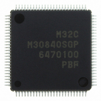
M30840SGP#U5 Renesas Electronics America, M30840SGP#U5 Datasheet - Page 222

M30840SGP#U5
Manufacturer Part Number
M30840SGP#U5
Description
IC M32C/84 MCU ROMLESS 100LQFP
Manufacturer
Renesas Electronics America
Series
M16C™ M32C/80r
Datasheet
1.M30843FWGPU5.pdf
(531 pages)
Specifications of M30840SGP#U5
Core Processor
M32C/80
Core Size
16/32-Bit
Speed
32MHz
Connectivity
CAN, I²C, IEBus, SIO, UART/USART
Peripherals
DMA, PWM, WDT
Number Of I /o
45
Program Memory Type
ROMless
Ram Size
10K x 8
Voltage - Supply (vcc/vdd)
3 V ~ 5.5 V
Data Converters
A/D 10x10b, D/A 2x8b
Oscillator Type
Internal
Operating Temperature
-20°C ~ 85°C
Package / Case
100-LQFP
For Use With
R0K330879S001BE - KIT DEV RSK M32C/87R0K330879S000BE - KIT DEV RSK M32C/87
Lead Free Status / RoHS Status
Lead free / RoHS Compliant
Eeprom Size
-
Program Memory Size
-
Available stocks
Company
Part Number
Manufacturer
Quantity
Price
Part Number:
M30840SGP#U5M30840SGP#U3
Manufacturer:
Renesas Electronics America
Quantity:
10 000
- Current page: 222 of 531
- Download datasheet (4Mb)
M
R
R
e
E
3
. v
J
Figure 17.6 U0SMR2 to U4SMR2 Registers
2
0
C
1
9
0 .
8 /
B
0
1
4
0
3
G
J
6
u
o r
0 -
. l
UARTi Special Mode Register 2
b7
u
NOTES:
0
1
p
, 7
0
b6
1. Refer to Table 17.14.
2. The external clock synchronous function can be selected by combining the SU1HIM bit and the
1
(
2
M
SCLKDIV bit in the UiSMR register.
0
b5
3
0
5
2
b4
C
SCLKDIV bit in the
UiSMR Register
8 /
b3
Page 199
, 4
b2
0
0
1
M
3
b1
2
C
b0
f o
8 /
4
SU1HIM
4
Symbol
SWC2
) T
IICM2
9
SWC
SDHI
CSC
ALS
STC
Bit
5
Symbol
U0SMR2 to U4SMR2
SU1HIM bit in the
UiSMR2 Register
I
Clock Synchronous Bit
SCL Wait Output Bit
SDA Output Stop Bit
UARTi Initialize Bit
SCL Wait Output Bit 2
SDA Output Inhibit Bit
External Clock
Synchronous Enable Bit
2
C Mode Select Bit 2
0 or 1
Bit Name
0
1
(i=0 to 4)
0366
Address
16,
External Clock Synchronous Function
Selection
No synchronization
External clock divided by 2
Same division as the external clock
02E6
(Note 1)
0: Disabled
1: Enabled
0: Disabled
1: Enabled
0: Output
1: No output
0: Disabled
1: Enabled
0: Transfer clock
1: "L" output
0: Output
1: No output (high-impedance)
(Note 2)
16,
0336
16,
0326
Function
16,
02F6
16
After Reset
00
16
RW
RW
RW
RW
RW
RW
RW
RW
RW
17. Serial I/O
Related parts for M30840SGP#U5
Image
Part Number
Description
Manufacturer
Datasheet
Request
R

Part Number:
Description:
KIT STARTER FOR M16C/29
Manufacturer:
Renesas Electronics America
Datasheet:

Part Number:
Description:
KIT STARTER FOR R8C/2D
Manufacturer:
Renesas Electronics America
Datasheet:

Part Number:
Description:
R0K33062P STARTER KIT
Manufacturer:
Renesas Electronics America
Datasheet:

Part Number:
Description:
KIT STARTER FOR R8C/23 E8A
Manufacturer:
Renesas Electronics America
Datasheet:

Part Number:
Description:
KIT STARTER FOR R8C/25
Manufacturer:
Renesas Electronics America
Datasheet:

Part Number:
Description:
KIT STARTER H8S2456 SHARPE DSPLY
Manufacturer:
Renesas Electronics America
Datasheet:

Part Number:
Description:
KIT STARTER FOR R8C38C
Manufacturer:
Renesas Electronics America
Datasheet:

Part Number:
Description:
KIT STARTER FOR R8C35C
Manufacturer:
Renesas Electronics America
Datasheet:

Part Number:
Description:
KIT STARTER FOR R8CL3AC+LCD APPS
Manufacturer:
Renesas Electronics America
Datasheet:

Part Number:
Description:
KIT STARTER FOR RX610
Manufacturer:
Renesas Electronics America
Datasheet:

Part Number:
Description:
KIT STARTER FOR R32C/118
Manufacturer:
Renesas Electronics America
Datasheet:

Part Number:
Description:
KIT DEV RSK-R8C/26-29
Manufacturer:
Renesas Electronics America
Datasheet:

Part Number:
Description:
KIT STARTER FOR SH7124
Manufacturer:
Renesas Electronics America
Datasheet:

Part Number:
Description:
KIT STARTER FOR H8SX/1622
Manufacturer:
Renesas Electronics America
Datasheet:

Part Number:
Description:
KIT DEV FOR SH7203
Manufacturer:
Renesas Electronics America
Datasheet:


