DF2265TE13V Renesas Electronics America, DF2265TE13V Datasheet - Page 160
DF2265TE13V
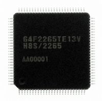
Manufacturer Part Number
DF2265TE13V
Description
IC H8S/2265 MCU FLASH 100TQFP
Manufacturer
Renesas Electronics America
Series
H8® H8S/2200r
Specifications of DF2265TE13V
Core Processor
H8S/2000
Core Size
16-Bit
Speed
13MHz
Connectivity
I²C, SCI, SmartCard
Peripherals
LCD, POR, PWM, WDT
Number Of I /o
67
Program Memory Size
128KB (128K x 8)
Program Memory Type
FLASH
Ram Size
4K x 8
Voltage - Supply (vcc/vdd)
3 V ~ 5.5 V
Data Converters
A/D 10x10b, D/A 2x8b
Oscillator Type
Internal
Operating Temperature
-20°C ~ 75°C
Package / Case
100-TQFP, 100-VQFP
Lead Free Status / RoHS Status
Lead free / RoHS Compliant
Eeprom Size
-
Available stocks
Company
Part Number
Manufacturer
Quantity
Price
Company:

Part Number:
DF2265TE13V
Manufacturer:
Renesas Electronics America
Quantity:
10 000


Section 6 PC Break Controller (PBC)
6.3.5
While the break interrupt enable bit is set to 1, instruction execution is one state later than usual.
• For 1-word branch instructions (Bcc d:8, BSR, JSR, JMP, TRAPA, RTE, and RTS) in on-chip
• When break interruption by instruction fetch is set, the set address indicates on-chip ROM or
• When break interruption by instruction fetch is set and a break interrupt is generated, if the
• When break interruption by instruction fetch is set and a break interrupt is generated, if the
Rev. 5.00 Sep. 01, 2009 Page 108 of 656
REJ09B0071-0500
Execution of instruction
after sleep instruction
After execution of the SLEEP instruction, a transition is made to the respective mode, and PC
break interrupt handling is not executed. However, the CMFA or CMFB flag is set (figure 6.2
(D)).
ROM or RAM.
RAM space, and that address is used for data access, the instruction that executes the data
access is one state later than in normal operation.
executing instruction immediately preceding the set instruction has one of the addressing
modes shown below, and that address indicates on-chip ROM or RAM, the instruction will be
one state later than in normal operation.
Addressing modes: @ERn, @(d:16,ERn), @(d:32,ERn), @-ERn/ERn+, @aa:8, @aa:24,
@aa:32, @(d:8,PC), @(d:16,PC), @@aa:8
executing instruction immediately preceding the set instruction is NOP or SLEEP, or has #xx,
Rn as its addressing mode, and that instruction is located in on-chip ROM or RAM, the
instruction will be one state later than in normal operation.
PC break exception
SLEEP instruction
execution
handling
When Instruction Execution Is Delayed by One State
(A)
Figure 6.2 Operation in Power-Down Mode Transitions
Execution of instruction
after sleep instruction
PC break exception
exception handling
SLEEP instruction
Direct transition
System clock
→ subclock
execution
handling
(B)
Subactive
mode
Execution of instruction
oscillation settling time
after sleep instruction
PC break exception
exception handling
SLEEP instruction
Direct transition
system clock,
Subclock →
execution
handling
(C)
High-speed
(medium-speed)
mode
SLEEP instruction
respective mode
Transition to
execution
(D)
Related parts for DF2265TE13V
Image
Part Number
Description
Manufacturer
Datasheet
Request
R

Part Number:
Description:
CONN SOCKET 2POS 7.92MM WHITE
Manufacturer:
Hirose Electric Co Ltd
Datasheet:

Part Number:
Description:
CONN SOCKET 4POS 7.92MM WHITE
Manufacturer:
Hirose Electric Co Ltd
Datasheet:

Part Number:
Description:
CONN SOCKET 5POS 7.92MM WHITE
Manufacturer:
Hirose Electric Co Ltd
Datasheet:

Part Number:
Description:
CONN SOCKET 3POS 7.92MM WHITE
Manufacturer:
Hirose Electric Co Ltd
Datasheet:
Part Number:
Description:
CONN SOCKET 5POS 7.92MM WHITE
Manufacturer:
Hirose Electric Co Ltd
Datasheet:

Part Number:
Description:
CONN SOCKET 2POS 7.92MM WHITE
Manufacturer:
Hirose Electric Co Ltd
Datasheet:
Part Number:
Description:
CONN SOCKET 3POS 7.92MM WHITE
Manufacturer:
Hirose Electric Co Ltd
Datasheet:
Part Number:
Description:
CONN SOCKET 4POS 7.92MM WHITE
Manufacturer:
Hirose Electric Co Ltd
Datasheet:

Part Number:
Description:
CONN HEADER 2POS 7.92MM R/A TIN
Manufacturer:
Hirose Electric Co Ltd
Datasheet:

Part Number:
Description:
CONN HEADER 4POS 7.92MM R/A TIN
Manufacturer:
Hirose Electric Co Ltd
Datasheet:

Part Number:
Description:
KIT STARTER FOR M16C/29
Manufacturer:
Renesas Electronics America
Datasheet:

Part Number:
Description:
KIT STARTER FOR R8C/2D
Manufacturer:
Renesas Electronics America
Datasheet:

Part Number:
Description:
R0K33062P STARTER KIT
Manufacturer:
Renesas Electronics America
Datasheet:

Part Number:
Description:
KIT STARTER FOR R8C/23 E8A
Manufacturer:
Renesas Electronics America
Datasheet:

Part Number:
Description:
KIT STARTER FOR R8C/25
Manufacturer:
Renesas Electronics America
Datasheet: