DF2265TE13V Renesas Electronics America, DF2265TE13V Datasheet - Page 41
DF2265TE13V
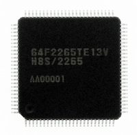
Manufacturer Part Number
DF2265TE13V
Description
IC H8S/2265 MCU FLASH 100TQFP
Manufacturer
Renesas Electronics America
Series
H8® H8S/2200r
Specifications of DF2265TE13V
Core Processor
H8S/2000
Core Size
16-Bit
Speed
13MHz
Connectivity
I²C, SCI, SmartCard
Peripherals
LCD, POR, PWM, WDT
Number Of I /o
67
Program Memory Size
128KB (128K x 8)
Program Memory Type
FLASH
Ram Size
4K x 8
Voltage - Supply (vcc/vdd)
3 V ~ 5.5 V
Data Converters
A/D 10x10b, D/A 2x8b
Oscillator Type
Internal
Operating Temperature
-20°C ~ 75°C
Package / Case
100-TQFP, 100-VQFP
Lead Free Status / RoHS Status
Lead free / RoHS Compliant
Eeprom Size
-
Available stocks
Company
Part Number
Manufacturer
Quantity
Price
Company:

Part Number:
DF2265TE13V
Manufacturer:
Renesas Electronics America
Quantity:
10 000


Figure 10.4 8-Bit Register Access Operation [Bus Master ↔ TCR (Upper 8 Bits)]................. 216
Figure 10.5 8-Bit Register Access Operation [Bus Master ↔ TMDR (Lower 8 Bits)]............. 217
Figure 10.6 8-Bit Register Access Operation [Bus Master ↔ TCR and TMDR (16 Bits)]....... 217
Figure 10.7 Example of Counter Operation Setting Procedure ................................................. 218
Figure 10.8 Free-Running Counter Operation ........................................................................... 219
Figure 10.9 Periodic Counter Operation.................................................................................... 220
Figure 10.10 Example of Setting Procedure for Waveform Output by Compare Match............. 220
Figure 10.11 Example of 0 Output/1 Output Operation .............................................................. 221
Figure 10.12 Example of Toggle Output Operation .................................................................... 221
Figure 10.13 Example of Input Capture Operation Setting Procedure ........................................ 222
Figure 10.14 Example of Input Capture Operation ..................................................................... 222
Figure 10.15 Example of Synchronous Operation Setting Procedure ......................................... 223
Figure 10.16 Example of Synchronous Operation....................................................................... 224
Figure 10.17 Compare Match Buffer Operation.......................................................................... 225
Figure 10.18 Input Capture Buffer Operation.............................................................................. 225
Figure 10.19 Example of Buffer Operation Setting Procedure.................................................... 226
Figure 10.20 Example of Buffer Operation (1) ........................................................................... 227
Figure 10.21 Example of Buffer Operation (2) ........................................................................... 228
Figure 10.22 Example of PWM Mode Setting Procedure ........................................................... 230
Figure 10.23 Example of PWM Mode Operation (1) .................................................................. 231
Figure 10.24 Example of PWM Mode Operation (2) .................................................................. 231
Figure 10.25 Example of PWM Mode Operation (3) .................................................................. 232
Figure 10.26 Example of Phase Counting Mode Setting Procedure............................................ 233
Figure 10.27 Example of Phase Counting Mode 1 Operation ..................................................... 234
Figure 10.28 Example of Phase Counting Mode 2 Operation ..................................................... 235
Figure 10.29 Example of Phase Counting Mode 3 Operation ..................................................... 236
Figure 10.30 Example of Phase Counting Mode 4 Operation ..................................................... 237
Figure 10.31 Count Timing in Internal Clock Operation............................................................. 240
Figure 10.32 Count Timing in External Clock Operation ........................................................... 240
Figure 10.33 Output Compare Output Timing ............................................................................ 241
Figure 10.34 Input Capture Input Signal Timing......................................................................... 241
Figure 10.35 Counter Clear Timing (Compare Match) ............................................................... 242
Figure 10.36 Counter Clear Timing (Input Capture) ................................................................... 242
Figure 10.37 Buffer Operation Timing (Compare Match) .......................................................... 243
Figure 10.38 Buffer Operation Timing (Input Capture) .............................................................. 243
Figure 10.39 TGI Interrupt Timing (Compare Match) ................................................................ 244
Figure 10.40 TGI Interrupt Timing (Input Capture) .................................................................... 245
Figure 10.41 TCIV Interrupt Setting Timing............................................................................... 245
Figure 10.42 TCIU Interrupt Setting Timing (H8S/2268 Group Only)....................................... 246
Figure 10.43 Timing for Status Flag Clearing by CPU ............................................................... 246
Figure 10.44 Timing for Status Flag Clearing by DTC Activation (H8S/2268 Group Only)...... 247
Rev. 5.00 Sep. 01, 2009 Page xxxix of l
REJ09B0071-0500
Related parts for DF2265TE13V
Image
Part Number
Description
Manufacturer
Datasheet
Request
R

Part Number:
Description:
CONN SOCKET 2POS 7.92MM WHITE
Manufacturer:
Hirose Electric Co Ltd
Datasheet:

Part Number:
Description:
CONN SOCKET 4POS 7.92MM WHITE
Manufacturer:
Hirose Electric Co Ltd
Datasheet:

Part Number:
Description:
CONN SOCKET 5POS 7.92MM WHITE
Manufacturer:
Hirose Electric Co Ltd
Datasheet:

Part Number:
Description:
CONN SOCKET 3POS 7.92MM WHITE
Manufacturer:
Hirose Electric Co Ltd
Datasheet:
Part Number:
Description:
CONN SOCKET 5POS 7.92MM WHITE
Manufacturer:
Hirose Electric Co Ltd
Datasheet:

Part Number:
Description:
CONN SOCKET 2POS 7.92MM WHITE
Manufacturer:
Hirose Electric Co Ltd
Datasheet:
Part Number:
Description:
CONN SOCKET 3POS 7.92MM WHITE
Manufacturer:
Hirose Electric Co Ltd
Datasheet:
Part Number:
Description:
CONN SOCKET 4POS 7.92MM WHITE
Manufacturer:
Hirose Electric Co Ltd
Datasheet:

Part Number:
Description:
CONN HEADER 2POS 7.92MM R/A TIN
Manufacturer:
Hirose Electric Co Ltd
Datasheet:

Part Number:
Description:
CONN HEADER 4POS 7.92MM R/A TIN
Manufacturer:
Hirose Electric Co Ltd
Datasheet:

Part Number:
Description:
KIT STARTER FOR M16C/29
Manufacturer:
Renesas Electronics America
Datasheet:

Part Number:
Description:
KIT STARTER FOR R8C/2D
Manufacturer:
Renesas Electronics America
Datasheet:

Part Number:
Description:
R0K33062P STARTER KIT
Manufacturer:
Renesas Electronics America
Datasheet:

Part Number:
Description:
KIT STARTER FOR R8C/23 E8A
Manufacturer:
Renesas Electronics America
Datasheet:

Part Number:
Description:
KIT STARTER FOR R8C/25
Manufacturer:
Renesas Electronics America
Datasheet: