DF2265TE13V Renesas Electronics America, DF2265TE13V Datasheet - Page 482
DF2265TE13V
Manufacturer Part Number
DF2265TE13V
Description
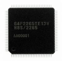
IC H8S/2265 MCU FLASH 100TQFP
Manufacturer
Renesas Electronics America
Series
H8® H8S/2200r
Specifications of DF2265TE13V
Core Processor
H8S/2000
Core Size
16-Bit
Speed
13MHz
Connectivity
I²C, SCI, SmartCard
Peripherals
LCD, POR, PWM, WDT
Number Of I /o
67
Program Memory Size
128KB (128K x 8)
Program Memory Type
FLASH
Ram Size
4K x 8
Voltage - Supply (vcc/vdd)
3 V ~ 5.5 V
Data Converters
A/D 10x10b, D/A 2x8b
Oscillator Type
Internal
Operating Temperature
-20°C ~ 75°C
Package / Case
100-TQFP, 100-VQFP
Lead Free Status / RoHS Status
Lead free / RoHS Compliant
Eeprom Size
-
Available stocks
Company
Part Number
Manufacturer
Quantity
Price
Company:

Part Number:
DF2265TE13V
Manufacturer:
Renesas Electronics America
Quantity:
10 000


Section 14 I
Table 14.7 I
4. SCL and SDA inputs are sampled in synchronization with the internal clock. The AC timing
5. The I
Rev. 5.00 Sep. 01, 2009 Page 430 of 656
REJ09B0071-0500
Item
SCL output cycle time
SCL output high pulse width
SCL output low pulse width
SDA output bus free time
Start condition output hold time
Retransmission start condition output
setup time
Stop condition output setup time
Data output setup time (master)
Data output setup time (slave)
Data output hold time
therefore depends on the system clock cycle t
interface AC timing specifications will not be met with a system clock frequency of less than 5
MHz.
speed mode). In master mode, the I
one bit at a time during communication. If t
the time determined by the input clock of the I
extended. The SCL rise time is determined by the pull-up resistance and load capacitance of
the SCL line. To insure proper operation at the set transfer rate, adjust the pull-up resistance
and load capacitance so that the SCL rise time does not exceed the values given in the table in
table 14.8.
2
C bus interface specification for the SCL rise time t
2
C Bus Interface (IIC) (Supported as an Option by H8S/2264 Group)
2
C Bus Timing (SCL and SDA Output)
2
C bus interface monitors the SCL line and synchronizes
Symbol
t
t
t
t
t
t
t
t
t
SCLO
SCLHO
SCLLO
BUFO
STAHO
STASO
STOSO
SDASO
SDAHO
sr
(the time for SCL to go from low to V
cyc
2
C bus interface, the high period of SCL is
, as shown in table 25.8. Note that the I
Output Timing
28 t
0.5 t
0.5 t
0.5 t
0.5 t
1 t
0.5 t
1 t
1 t
3 t
SCLO
SCLLO
SCLL
cyc
cyc
SCLO
SCLO
SCLO
SCLO
SCLO
– 3 t
to 256 t
sr
– 3 t
is under 1000 ns (300 ns for high-
– 1 t
– 1 t
+ 2 t
cyc
cyc
cyc
cyc
cyc
cyc
Unit
ns
ns
ns
ns
ns
ns
ns
ns
ns
ns
Notes
IH
) exceeds
2
C bus
Related parts for DF2265TE13V
Image
Part Number
Description
Manufacturer
Datasheet
Request
R

Part Number:
Description:
CONN SOCKET 2POS 7.92MM WHITE
Manufacturer:
Hirose Electric Co Ltd
Datasheet:

Part Number:
Description:
CONN SOCKET 4POS 7.92MM WHITE
Manufacturer:
Hirose Electric Co Ltd
Datasheet:

Part Number:
Description:
CONN SOCKET 5POS 7.92MM WHITE
Manufacturer:
Hirose Electric Co Ltd
Datasheet:

Part Number:
Description:
CONN SOCKET 3POS 7.92MM WHITE
Manufacturer:
Hirose Electric Co Ltd
Datasheet:
Part Number:
Description:
CONN SOCKET 5POS 7.92MM WHITE
Manufacturer:
Hirose Electric Co Ltd
Datasheet:

Part Number:
Description:
CONN SOCKET 2POS 7.92MM WHITE
Manufacturer:
Hirose Electric Co Ltd
Datasheet:
Part Number:
Description:
CONN SOCKET 3POS 7.92MM WHITE
Manufacturer:
Hirose Electric Co Ltd
Datasheet:
Part Number:
Description:
CONN SOCKET 4POS 7.92MM WHITE
Manufacturer:
Hirose Electric Co Ltd
Datasheet:

Part Number:
Description:
CONN HEADER 2POS 7.92MM R/A TIN
Manufacturer:
Hirose Electric Co Ltd
Datasheet:

Part Number:
Description:
CONN HEADER 4POS 7.92MM R/A TIN
Manufacturer:
Hirose Electric Co Ltd
Datasheet:

Part Number:
Description:
KIT STARTER FOR M16C/29
Manufacturer:
Renesas Electronics America
Datasheet:

Part Number:
Description:
KIT STARTER FOR R8C/2D
Manufacturer:
Renesas Electronics America
Datasheet:

Part Number:
Description:
R0K33062P STARTER KIT
Manufacturer:
Renesas Electronics America
Datasheet:

Part Number:
Description:
KIT STARTER FOR R8C/23 E8A
Manufacturer:
Renesas Electronics America
Datasheet:

Part Number:
Description:
KIT STARTER FOR R8C/25
Manufacturer:
Renesas Electronics America
Datasheet: