DF2265TE13V Renesas Electronics America, DF2265TE13V Datasheet - Page 415
DF2265TE13V
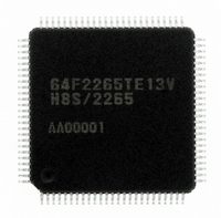
Manufacturer Part Number
DF2265TE13V
Description
IC H8S/2265 MCU FLASH 100TQFP
Manufacturer
Renesas Electronics America
Series
H8® H8S/2200r
Specifications of DF2265TE13V
Core Processor
H8S/2000
Core Size
16-Bit
Speed
13MHz
Connectivity
I²C, SCI, SmartCard
Peripherals
LCD, POR, PWM, WDT
Number Of I /o
67
Program Memory Size
128KB (128K x 8)
Program Memory Type
FLASH
Ram Size
4K x 8
Voltage - Supply (vcc/vdd)
3 V ~ 5.5 V
Data Converters
A/D 10x10b, D/A 2x8b
Oscillator Type
Internal
Operating Temperature
-20°C ~ 75°C
Package / Case
100-TQFP, 100-VQFP
Lead Free Status / RoHS Status
Lead free / RoHS Compliant
Eeprom Size
-
Available stocks
Company
Part Number
Manufacturer
Quantity
Price
Company:

Part Number:
DF2265TE13V
Manufacturer:
Renesas Electronics America
Quantity:
10 000


13.7
The SCI supports an IC card (Smart Card) interface that conforms to ISO/IEC 7816-3
(Identification Card) as a serial communication interface extension function. Switching between
the normal serial communication interface and the Smart Card interface mode is carried out by
means of a register setting.
13.7.1
Figure 13.24 shows an example of connection with the Smart Card. In communication with an IC
card, as both transmission and reception are carried out on a single data transmission line, the TxD
pin and RxD pin should be connected to the LSI pin. The data transmission line should be pulled
up to the V
are both set to 1, closed transmission/reception is possible, enabling self-diagnosis to be carried
out. When the clock generated on the Smart Card interface is used by an IC card, the SCK pin
output is input to the CLK pin of the IC card. This LSI port output is used as the reset signal.
13.7.2
Figure 13.25 shows the transfer data format in Smart Card interface mode.
• One frame consists of 8-bit data plus a parity bit in asynchronous mode.
• In transmission, a guard time of at least 2 etu (Elementary Time Unit: the time for transfer of
• If a parity error is detected during reception, a low error signal level is output for one etu
• If an error signal is sampled during transmission, the same data is retransmitted automatically
one bit) is left between the end of the parity bit and the start of the next frame.
period, 10.5 etu after the start bit.
after a delay of 2 etu or longer.
Operation in Smart Card Interface
Figure 13.24 Schematic Diagram of Smart Card Interface Pin Connections
Pin Connection Example
Data Format (Except for Block Transfer Mode)
CC
power supply with a resistor. If an IC card is not connected, and the TE and RE bits
Connected equipment
This LSI
Px (port)
SCK
RxD
TxD
Section 13 Serial Communication Interface (SCI)
Data line
Clock line
Reset line
V
CC
Rev. 5.00 Sep. 01, 2009 Page 363 of 656
I/O
CLK
RST
IC card
REJ09B0071-0500
Related parts for DF2265TE13V
Image
Part Number
Description
Manufacturer
Datasheet
Request
R

Part Number:
Description:
CONN SOCKET 2POS 7.92MM WHITE
Manufacturer:
Hirose Electric Co Ltd
Datasheet:

Part Number:
Description:
CONN SOCKET 4POS 7.92MM WHITE
Manufacturer:
Hirose Electric Co Ltd
Datasheet:

Part Number:
Description:
CONN SOCKET 5POS 7.92MM WHITE
Manufacturer:
Hirose Electric Co Ltd
Datasheet:

Part Number:
Description:
CONN SOCKET 3POS 7.92MM WHITE
Manufacturer:
Hirose Electric Co Ltd
Datasheet:
Part Number:
Description:
CONN SOCKET 5POS 7.92MM WHITE
Manufacturer:
Hirose Electric Co Ltd
Datasheet:

Part Number:
Description:
CONN SOCKET 2POS 7.92MM WHITE
Manufacturer:
Hirose Electric Co Ltd
Datasheet:
Part Number:
Description:
CONN SOCKET 3POS 7.92MM WHITE
Manufacturer:
Hirose Electric Co Ltd
Datasheet:
Part Number:
Description:
CONN SOCKET 4POS 7.92MM WHITE
Manufacturer:
Hirose Electric Co Ltd
Datasheet:

Part Number:
Description:
CONN HEADER 2POS 7.92MM R/A TIN
Manufacturer:
Hirose Electric Co Ltd
Datasheet:

Part Number:
Description:
CONN HEADER 4POS 7.92MM R/A TIN
Manufacturer:
Hirose Electric Co Ltd
Datasheet:

Part Number:
Description:
KIT STARTER FOR M16C/29
Manufacturer:
Renesas Electronics America
Datasheet:

Part Number:
Description:
KIT STARTER FOR R8C/2D
Manufacturer:
Renesas Electronics America
Datasheet:

Part Number:
Description:
R0K33062P STARTER KIT
Manufacturer:
Renesas Electronics America
Datasheet:

Part Number:
Description:
KIT STARTER FOR R8C/23 E8A
Manufacturer:
Renesas Electronics America
Datasheet:

Part Number:
Description:
KIT STARTER FOR R8C/25
Manufacturer:
Renesas Electronics America
Datasheet: