DF2265TE13V Renesas Electronics America, DF2265TE13V Datasheet - Page 49
DF2265TE13V
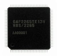
Manufacturer Part Number
DF2265TE13V
Description
IC H8S/2265 MCU FLASH 100TQFP
Manufacturer
Renesas Electronics America
Series
H8® H8S/2200r
Specifications of DF2265TE13V
Core Processor
H8S/2000
Core Size
16-Bit
Speed
13MHz
Connectivity
I²C, SCI, SmartCard
Peripherals
LCD, POR, PWM, WDT
Number Of I /o
67
Program Memory Size
128KB (128K x 8)
Program Memory Type
FLASH
Ram Size
4K x 8
Voltage - Supply (vcc/vdd)
3 V ~ 5.5 V
Data Converters
A/D 10x10b, D/A 2x8b
Oscillator Type
Internal
Operating Temperature
-20°C ~ 75°C
Package / Case
100-TQFP, 100-VQFP
Lead Free Status / RoHS Status
Lead free / RoHS Compliant
Eeprom Size
-
Available stocks
Company
Part Number
Manufacturer
Quantity
Price
Company:

Part Number:
DF2265TE13V
Manufacturer:
Renesas Electronics America
Quantity:
10 000


Table 5.8
Table 5.9
Section 8 Data Transfer Controller (DTC)
Table 8.1
Table 8.2
Table 8.3
Table 8.4
Table 8.5
Table 8.6
Table 8.7
Section 9 I/O Ports
Table 9.1
Table 9.1
Table 9.2
Table 9.3
Section 10 16-Bit Timer Pulse Unit (TPU)
Table 10.1
Table 10.2
Table 10.3
Table 10.4
Table 10.5
Table 10.6
Table 10.7
Table 10.8
Table 10.9
Table 10.10 TIORL_0 (Channel 0) (H8S/2268 Group Only) .................................................... 200
Table 10.11 TIOR_1 (Channel 1)............................................................................................... 201
Table 10.12 TIOR_2 (Channel 2)............................................................................................... 202
Table 10.13 TIORH_0 (Channel 0) (H8S/2268 Group Only) .................................................... 203
Table 10.14 TIORL_0 (Channel 0) (H8S/2268 Group Only) .................................................... 204
Table 10.15 TIOR_1 (Channel 1)............................................................................................... 205
Table 10.16 TIOR_2 (Channel 2)............................................................................................... 206
Table 10.17 Register Combinations in Buffer Operation........................................................... 225
Table 10.18 PWM Output Registers and Output Pins................................................................ 229
Table 10.19 Phase Counting Mode Clock Input Pins................................................................. 233
Table 10.20 Up/Down-Count Conditions in Phase Counting Mode 1 ....................................... 234
Table 10.21 Up/Down-Count Conditions in Phase Counting Mode 2 ....................................... 235
Table 10.22 Up/Down-Count Conditions in Phase Counting Mode 3 ....................................... 236
Number of States in Interrupt Handling Routine Execution Status..........................98
Interrupt Source Selection and Clear Control......................................................... 100
Activation Source and DTCER Clearing................................................................ 122
Interrupt Sources, DTC Vector Addresses, and Corresponding DTCEs ................ 125
Register Information in Normal Mode ................................................................... 128
Register Information in Repeat Mode .................................................................... 129
Register Information in Block Transfer Mode ....................................................... 130
DTC Execution Status ............................................................................................ 134
Number of States Required for Each Execution Status .......................................... 134
H8S/2268 Group Port Functions (1)....................................................................... 140
H8S/2264 Group Port Functions (2)....................................................................... 143
Input Pull-Up MOS States (Port J)......................................................................... 173
Examples of Ways to Handle Unused Input Pins................................................... 184
TPU Functions........................................................................................................ 186
TPU Pins ................................................................................................................ 190
CCLR0 to CCLR2 (Channel 0) (H8S/2268 Group Only) ...................................... 193
CCLR0 to CCLR2 (Channels 1 and 2)................................................................... 193
TPSC0 to TPSC2 (Channel 0) (H8S/2268 Group Only) ........................................ 194
TPSC0 to TPSC2 (Channel 1)................................................................................ 194
TPSC0 to TPSC2 (Channel 2)................................................................................ 195
MD0 to MD3.......................................................................................................... 197
TIORH_0 (Channel 0) (H8S/2268 Group Only) .................................................... 199
Rev. 5.00 Sep. 01, 2009 Page xlvii of l
REJ09B0071-0500
Related parts for DF2265TE13V
Image
Part Number
Description
Manufacturer
Datasheet
Request
R

Part Number:
Description:
CONN SOCKET 2POS 7.92MM WHITE
Manufacturer:
Hirose Electric Co Ltd
Datasheet:

Part Number:
Description:
CONN SOCKET 4POS 7.92MM WHITE
Manufacturer:
Hirose Electric Co Ltd
Datasheet:

Part Number:
Description:
CONN SOCKET 5POS 7.92MM WHITE
Manufacturer:
Hirose Electric Co Ltd
Datasheet:

Part Number:
Description:
CONN SOCKET 3POS 7.92MM WHITE
Manufacturer:
Hirose Electric Co Ltd
Datasheet:
Part Number:
Description:
CONN SOCKET 5POS 7.92MM WHITE
Manufacturer:
Hirose Electric Co Ltd
Datasheet:

Part Number:
Description:
CONN SOCKET 2POS 7.92MM WHITE
Manufacturer:
Hirose Electric Co Ltd
Datasheet:
Part Number:
Description:
CONN SOCKET 3POS 7.92MM WHITE
Manufacturer:
Hirose Electric Co Ltd
Datasheet:
Part Number:
Description:
CONN SOCKET 4POS 7.92MM WHITE
Manufacturer:
Hirose Electric Co Ltd
Datasheet:

Part Number:
Description:
CONN HEADER 2POS 7.92MM R/A TIN
Manufacturer:
Hirose Electric Co Ltd
Datasheet:

Part Number:
Description:
CONN HEADER 4POS 7.92MM R/A TIN
Manufacturer:
Hirose Electric Co Ltd
Datasheet:

Part Number:
Description:
KIT STARTER FOR M16C/29
Manufacturer:
Renesas Electronics America
Datasheet:

Part Number:
Description:
KIT STARTER FOR R8C/2D
Manufacturer:
Renesas Electronics America
Datasheet:

Part Number:
Description:
R0K33062P STARTER KIT
Manufacturer:
Renesas Electronics America
Datasheet:

Part Number:
Description:
KIT STARTER FOR R8C/23 E8A
Manufacturer:
Renesas Electronics America
Datasheet:

Part Number:
Description:
KIT STARTER FOR R8C/25
Manufacturer:
Renesas Electronics America
Datasheet: