DF2265TE13V Renesas Electronics America, DF2265TE13V Datasheet - Page 585
DF2265TE13V
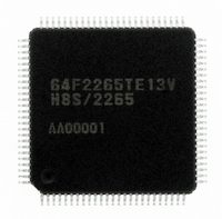
Manufacturer Part Number
DF2265TE13V
Description
IC H8S/2265 MCU FLASH 100TQFP
Manufacturer
Renesas Electronics America
Series
H8® H8S/2200r
Specifications of DF2265TE13V
Core Processor
H8S/2000
Core Size
16-Bit
Speed
13MHz
Connectivity
I²C, SCI, SmartCard
Peripherals
LCD, POR, PWM, WDT
Number Of I /o
67
Program Memory Size
128KB (128K x 8)
Program Memory Type
FLASH
Ram Size
4K x 8
Voltage - Supply (vcc/vdd)
3 V ~ 5.5 V
Data Converters
A/D 10x10b, D/A 2x8b
Oscillator Type
Internal
Operating Temperature
-20°C ~ 75°C
Package / Case
100-TQFP, 100-VQFP
Lead Free Status / RoHS Status
Lead free / RoHS Compliant
Eeprom Size
-
Available stocks
Company
Part Number
Manufacturer
Quantity
Price
Company:

Part Number:
DF2265TE13V
Manufacturer:
Renesas Electronics America
Quantity:
10 000


20.13
Precautions concerning the use of on-board programming mode, the RAM emulation function, and
programmer mode are summarized below.
Use the specified voltages and timing for programming and erasing: Applied voltages in
excess of the rating can permanently damage the device. Use a PROM programmer that supports
the Renesas 256-kbyte flash memory on-chip microcomputer device type (FZTAT256V3A).
Do not select the HN27C4096 setting for the PROM programmer, and only use the specified
socket adapter. Failure to observe these points may result in damage to the device.
Powering on and off (see figures 20.13 to 20.15): Do not apply a high level to the FWE pin until
VCC has stabilized. Also, drive the FWE pin low before turning off VCC.
When applying or disconnecting VCC power, fix the FWE pin low and place the flash memory in
the hardware protection state.
The power-on and power-off timing requirements should also be satisfied in the event of a power
failure and subsequent recovery.
FWE application/disconnection (see figures 20.13 to 20.15): FWE application should be carried
out when MCU operation is in a stable condition. If MCU operation is not stable, fix the FWE pin
low and set the protection state.
The following points must be observed concerning FWE application and disconnection to prevent
unintentional programming or erasing of flash memory:
• Apply FWE when the VCC voltage has stabilized within its rated voltage range.
• In boot mode, apply and disconnect FWE during a reset.
• In user program mode, FWE can be switched between high and low level regardless of the
• Do not apply FWE if program runaway has occurred.
• Disconnect FWE only when the SWE1, ESU1, PSU1, EV1, PV1, P1, and E1 bits in FLMCR1
reset state. FWE input can also be switched during execution of a program in flash memory.
are cleared.
Make sure that the SWE1, ESU1, PSU1, EV1, PV1, P1, and E1 bits are not set by mistake
when applying or disconnecting FWE.
Flash Memory Programming and Erasing Precautions
Rev. 5.00 Sep. 01, 2009 Page 533 of 656
REJ09B0071-0500
Section 20 ROM
Related parts for DF2265TE13V
Image
Part Number
Description
Manufacturer
Datasheet
Request
R

Part Number:
Description:
CONN SOCKET 2POS 7.92MM WHITE
Manufacturer:
Hirose Electric Co Ltd
Datasheet:

Part Number:
Description:
CONN SOCKET 4POS 7.92MM WHITE
Manufacturer:
Hirose Electric Co Ltd
Datasheet:

Part Number:
Description:
CONN SOCKET 5POS 7.92MM WHITE
Manufacturer:
Hirose Electric Co Ltd
Datasheet:

Part Number:
Description:
CONN SOCKET 3POS 7.92MM WHITE
Manufacturer:
Hirose Electric Co Ltd
Datasheet:
Part Number:
Description:
CONN SOCKET 5POS 7.92MM WHITE
Manufacturer:
Hirose Electric Co Ltd
Datasheet:

Part Number:
Description:
CONN SOCKET 2POS 7.92MM WHITE
Manufacturer:
Hirose Electric Co Ltd
Datasheet:
Part Number:
Description:
CONN SOCKET 3POS 7.92MM WHITE
Manufacturer:
Hirose Electric Co Ltd
Datasheet:
Part Number:
Description:
CONN SOCKET 4POS 7.92MM WHITE
Manufacturer:
Hirose Electric Co Ltd
Datasheet:

Part Number:
Description:
CONN HEADER 2POS 7.92MM R/A TIN
Manufacturer:
Hirose Electric Co Ltd
Datasheet:

Part Number:
Description:
CONN HEADER 4POS 7.92MM R/A TIN
Manufacturer:
Hirose Electric Co Ltd
Datasheet:

Part Number:
Description:
KIT STARTER FOR M16C/29
Manufacturer:
Renesas Electronics America
Datasheet:

Part Number:
Description:
KIT STARTER FOR R8C/2D
Manufacturer:
Renesas Electronics America
Datasheet:

Part Number:
Description:
R0K33062P STARTER KIT
Manufacturer:
Renesas Electronics America
Datasheet:

Part Number:
Description:
KIT STARTER FOR R8C/23 E8A
Manufacturer:
Renesas Electronics America
Datasheet:

Part Number:
Description:
KIT STARTER FOR R8C/25
Manufacturer:
Renesas Electronics America
Datasheet: