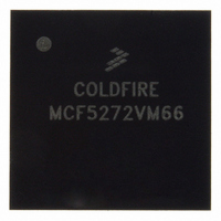
MCF5272VM66 Freescale Semiconductor, MCF5272VM66 Datasheet - Page 190

MCF5272VM66
Manufacturer Part Number
MCF5272VM66
Description
IC MPU 66MHZ COLDFIRE 196-MAPBGA
Manufacturer
Freescale Semiconductor
Series
MCF527xr
Specifications of MCF5272VM66
Core Processor
Coldfire V2
Core Size
32-Bit
Speed
66MHz
Connectivity
EBI/EMI, Ethernet, I²C, SPI, UART/USART, USB
Peripherals
DMA, WDT
Number Of I /o
32
Program Memory Size
16KB (4K x 32)
Program Memory Type
ROM
Ram Size
1K x 32
Voltage - Supply (vcc/vdd)
3 V ~ 3.6 V
Oscillator Type
External
Operating Temperature
0°C ~ 70°C
Package / Case
196-MAPBGA
Family Name
MCF5xxx
Device Core
ColdFire
Device Core Size
32b
Frequency (max)
66MHz
Instruction Set Architecture
RISC
Supply Voltage 1 (typ)
3.3V
Operating Temp Range
0C to 70C
Operating Temperature Classification
Commercial
Mounting
Surface Mount
Pin Count
196
Package Type
MA-BGA
Cpu Speed
66MHz
Embedded Interface Type
UART, QSPI, USB, TDM
Digital Ic Case Style
BGA
No. Of Pins
196
Supply Voltage Range
3V To 3.6V
Rohs Compliant
Yes
Lead Free Status / RoHS Status
Lead free / RoHS Compliant
Eeprom Size
-
Data Converters
-
Lead Free Status / Rohs Status
Compliant
Available stocks
Company
Part Number
Manufacturer
Quantity
Price
Company:
Part Number:
MCF5272VM66
Manufacturer:
FREESCAL
Quantity:
30 000
Company:
Part Number:
MCF5272VM66
Manufacturer:
MOTOLOLA
Quantity:
648
Company:
Part Number:
MCF5272VM66
Manufacturer:
Freescale Semiconductor
Quantity:
10 000
Part Number:
MCF5272VM66
Manufacturer:
MOTOROLA/摩托罗拉
Quantity:
20 000
Part Number:
MCF5272VM66 K75N
Manufacturer:
FREESCALE
Quantity:
20 000
Company:
Part Number:
MCF5272VM66J
Manufacturer:
FREESCAL
Quantity:
416
Company:
Part Number:
MCF5272VM66J
Manufacturer:
Freescale
Quantity:
178
Company:
Part Number:
MCF5272VM66J
Manufacturer:
Freescale Semiconductor
Quantity:
10 000
Company:
Part Number:
MCF5272VM66K75N
Manufacturer:
Freescal
Quantity:
18
Company:
Part Number:
MCF5272VM66R2
Manufacturer:
Freescale Semiconductor
Quantity:
10 000
Company:
Part Number:
MCF5272VM66R2J
Manufacturer:
Freescale Semiconductor
Quantity:
10 000
- Current page: 190 of 544
- Download datasheet (7Mb)
Chip Select Module
8-6
Name
6–2
9
8
7
1
0
EXTBURST Enable extended burst. Valid only for CS7. Reserved bit for CS[0:5]. EXTBURST should be 1 when
RDAH
Name
MRW
WS
RW
—
Controls the address and attribute hold time after the termination, internal or external with TA, of a read
cycle that hits in the chip select address space.
0 Do not hold address and attribute signals an extra cycle after chip select negates on reads.
1 Hold address and attribute signals an extra cycle after chip select negate on reads.
external SDRAM is configured for a data bus narrower than the width programmed for the MCF5272.
EBI must be set for SDRAM and the BW must be set to the data bus width of the external SDRAM array.
Example: If the MCF5272 external physical data bus width is 32 or 16 bits but the external SDRAM is
16 bits wide, EXTBURST must be set and BW must be 10 (word) for SDCS.
0 Extended bursts are not enabled.
1 Extended bursts are enabled.
Reserved, should be cleared.
Wait state generator. Specifies the number of wait states (in system clocks) needed before the SIM
generates an internal transfer acknowledge signal to terminate the access.
0x00 No wait states
0x01 1 wait state
...
0x1E 30 wait states
0x1F External access
For example, WS = 0x0A introduces a 10-clock wait before the bus cycle terminates; 0x1F indicates a
source external to the chip select module terminates the access.
For SRAM and ROM accesses EBI codes 00 or 11 and WS = 0x1F, TA must be driven from an external
source to terminate the bus cycle, otherwise the on-chip bus timeout monitor issues a bus error
exception.
For SRAM and ROM accesses with EBI = 00 or 11 and WS = 0x00–0x1E, the chip select module
terminates the bus cycle after the programmed number of system clocks.
For SDRAM accesses with SDCS, EBI = 01, and WS = 0x1F, bus cycles are terminated under control
of the SDRAM controller.
The CSOR0[WS] reset default is 0x1E. The default for all other CSORs is 0x00.
Caution: Never drive TA as an input to terminate SDRAM peripheral accesses.
RW and MRW determine whether the selected memory region is read only or write only.
0 Read only
1 Write only
MRW must be set for value of RW be taken into consideration.
0 Memory covered by chip select is read/write. The memory covered by the chip select is neither read
1 RW determines whether memory covered by chip select is read only or write only. A conflict causes
MCF5272 ColdFire
nor write protected.
either a read or write protect violation.
Table 8-5. CSORn Field Descriptions (continued)
®
Integrated Microprocessor User’s Manual, Rev. 3
Description
Freescale Semiconductor
Related parts for MCF5272VM66
Image
Part Number
Description
Manufacturer
Datasheet
Request
R
Part Number:
Description:
Mcf5272 Coldfire Integrated Microprocessor User
Manufacturer:
Freescale Semiconductor, Inc
Datasheet:

Part Number:
Description:
MCF5272 Interrupt Service Routine for the Physical Layer Interface Controller
Manufacturer:
Freescale Semiconductor / Motorola
Datasheet:
Part Number:
Description:
Manufacturer:
Freescale Semiconductor, Inc
Datasheet:
Part Number:
Description:
Manufacturer:
Freescale Semiconductor, Inc
Datasheet:
Part Number:
Description:
Manufacturer:
Freescale Semiconductor, Inc
Datasheet:
Part Number:
Description:
Manufacturer:
Freescale Semiconductor, Inc
Datasheet:
Part Number:
Description:
Manufacturer:
Freescale Semiconductor, Inc
Datasheet:
Part Number:
Description:
Manufacturer:
Freescale Semiconductor, Inc
Datasheet:
Part Number:
Description:
Manufacturer:
Freescale Semiconductor, Inc
Datasheet:
Part Number:
Description:
Manufacturer:
Freescale Semiconductor, Inc
Datasheet:
Part Number:
Description:
Manufacturer:
Freescale Semiconductor, Inc
Datasheet:
Part Number:
Description:
Manufacturer:
Freescale Semiconductor, Inc
Datasheet:
Part Number:
Description:
Manufacturer:
Freescale Semiconductor, Inc
Datasheet:
Part Number:
Description:
Manufacturer:
Freescale Semiconductor, Inc
Datasheet:
Part Number:
Description:
Manufacturer:
Freescale Semiconductor, Inc
Datasheet:


