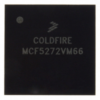
MCF5272VM66 Freescale Semiconductor, MCF5272VM66 Datasheet - Page 235

MCF5272VM66
Manufacturer Part Number
MCF5272VM66
Description
IC MPU 66MHZ COLDFIRE 196-MAPBGA
Manufacturer
Freescale Semiconductor
Series
MCF527xr
Specifications of MCF5272VM66
Core Processor
Coldfire V2
Core Size
32-Bit
Speed
66MHz
Connectivity
EBI/EMI, Ethernet, I²C, SPI, UART/USART, USB
Peripherals
DMA, WDT
Number Of I /o
32
Program Memory Size
16KB (4K x 32)
Program Memory Type
ROM
Ram Size
1K x 32
Voltage - Supply (vcc/vdd)
3 V ~ 3.6 V
Oscillator Type
External
Operating Temperature
0°C ~ 70°C
Package / Case
196-MAPBGA
Family Name
MCF5xxx
Device Core
ColdFire
Device Core Size
32b
Frequency (max)
66MHz
Instruction Set Architecture
RISC
Supply Voltage 1 (typ)
3.3V
Operating Temp Range
0C to 70C
Operating Temperature Classification
Commercial
Mounting
Surface Mount
Pin Count
196
Package Type
MA-BGA
Cpu Speed
66MHz
Embedded Interface Type
UART, QSPI, USB, TDM
Digital Ic Case Style
BGA
No. Of Pins
196
Supply Voltage Range
3V To 3.6V
Rohs Compliant
Yes
Lead Free Status / RoHS Status
Lead free / RoHS Compliant
Eeprom Size
-
Data Converters
-
Lead Free Status / Rohs Status
Compliant
Available stocks
Company
Part Number
Manufacturer
Quantity
Price
Company:
Part Number:
MCF5272VM66
Manufacturer:
FREESCAL
Quantity:
30 000
Company:
Part Number:
MCF5272VM66
Manufacturer:
MOTOLOLA
Quantity:
648
Company:
Part Number:
MCF5272VM66
Manufacturer:
Freescale Semiconductor
Quantity:
10 000
Part Number:
MCF5272VM66
Manufacturer:
MOTOROLA/摩托罗拉
Quantity:
20 000
Part Number:
MCF5272VM66 K75N
Manufacturer:
FREESCALE
Quantity:
20 000
Company:
Part Number:
MCF5272VM66J
Manufacturer:
FREESCAL
Quantity:
416
Company:
Part Number:
MCF5272VM66J
Manufacturer:
Freescale
Quantity:
178
Company:
Part Number:
MCF5272VM66J
Manufacturer:
Freescale Semiconductor
Quantity:
10 000
Company:
Part Number:
MCF5272VM66K75N
Manufacturer:
Freescal
Quantity:
18
Company:
Part Number:
MCF5272VM66R2
Manufacturer:
Freescale Semiconductor
Quantity:
10 000
Company:
Part Number:
MCF5272VM66R2J
Manufacturer:
Freescale Semiconductor
Quantity:
10 000
- Current page: 235 of 544
- Download datasheet (7Mb)
11.5.7
The MMFR register,
device(s), providing read/write access to their MII registers. Performing a write to the MMFR register
causes a management frame to be sourced, unless the MSCR register has been programmed to 0. In the
case of writing to MMFR when MSCR = 0, if the MSCR register is then written to a non-zero value, an
MII frame is generated with the data previously written to MMFR. This allows MMFR and MSCR to be
programmed in either order if MSCR is currently zero.
Table 11-13
To perform a read or write operation on the MII management interface, the MMFR register is written by
the user. To generate a valid read or write management frame, the ST field must be written with a 01
pattern, the OP field must be written with a 01 (management register write frame) or 10 (management
register read frame), and the TA field must be written with a 10. If other patterns are written to these fields,
a frame is generated but will not comply with the IEEE 802.3 MII definition. OP field = 1x produces a
read-frame operation, while OP = 0x produces a write-frame operation.
To generate an 802.3-compliant MII management interface write frame (write to a PHY register), the user
must write {01 01 PHYAD REGAD 10 DATA} to the MMFR register. Writing this pattern causes the
control logic to shift out the data in the MMFR register following a preamble generated by the control state
machine. The contents of MMFR are altered as the contents are serially shifted, and are unpredictable if
read by the user. Once the write management frame operation completes, the MII interrupt is generated.
At this time, the contents of the MMFR register match the original value written.
Freescale Semiconductor
31–30
29–28
27–23
22–18
17–16
15–0
Bits
Reset
Reset
Field
Field
Addr
R/W
R/W
Name
MII Management Frame Register (MMFR)
DATA
describes the MMFR fields.
31
15
OP
ST
RA
PA
TA
ST
30
Start of frame delimiter. Must be programmed to 01 for a valid MII management frame
Operation code. This field must be programmed to 10 (read) or 01(write) to generate a valid MII
management frame. A value of 11 produces a read frame operation while a value of 00 produces a
write frame operation, but these frames are not MII-compliant.
PHY address. Specifies one of up to 32 attached PHY devices
Register address. Specifies one of up to 32 registers within the specified PHY device
Turn around. Must be programmed to 10 to generate a valid MII management frame.
Management frame data. Field for data to be written to or read from PHY register
Figure
MCF5272 ColdFire
29
Figure 11-11. MII Management Frame Register (MMFR)
OP
11-11, is used to communicate with the attached MII compatible PHY
28
Table 11-13. MMFR Field Descriptions
27
®
Integrated Microprocessor User’s Manual, Rev. 3
PA
MBAR + 0x880
Read/Write
Read/Write
Undefined
Undefined
23
DATA
Description
22
RA
18
17
Ethernet Module
TA
16
0
11-17
Related parts for MCF5272VM66
Image
Part Number
Description
Manufacturer
Datasheet
Request
R
Part Number:
Description:
Mcf5272 Coldfire Integrated Microprocessor User
Manufacturer:
Freescale Semiconductor, Inc
Datasheet:

Part Number:
Description:
MCF5272 Interrupt Service Routine for the Physical Layer Interface Controller
Manufacturer:
Freescale Semiconductor / Motorola
Datasheet:
Part Number:
Description:
Manufacturer:
Freescale Semiconductor, Inc
Datasheet:
Part Number:
Description:
Manufacturer:
Freescale Semiconductor, Inc
Datasheet:
Part Number:
Description:
Manufacturer:
Freescale Semiconductor, Inc
Datasheet:
Part Number:
Description:
Manufacturer:
Freescale Semiconductor, Inc
Datasheet:
Part Number:
Description:
Manufacturer:
Freescale Semiconductor, Inc
Datasheet:
Part Number:
Description:
Manufacturer:
Freescale Semiconductor, Inc
Datasheet:
Part Number:
Description:
Manufacturer:
Freescale Semiconductor, Inc
Datasheet:
Part Number:
Description:
Manufacturer:
Freescale Semiconductor, Inc
Datasheet:
Part Number:
Description:
Manufacturer:
Freescale Semiconductor, Inc
Datasheet:
Part Number:
Description:
Manufacturer:
Freescale Semiconductor, Inc
Datasheet:
Part Number:
Description:
Manufacturer:
Freescale Semiconductor, Inc
Datasheet:
Part Number:
Description:
Manufacturer:
Freescale Semiconductor, Inc
Datasheet:
Part Number:
Description:
Manufacturer:
Freescale Semiconductor, Inc
Datasheet:


