IAR-KSK-IMX25 Freescale Semiconductor, IAR-KSK-IMX25 Datasheet - Page 33
IAR-KSK-IMX25
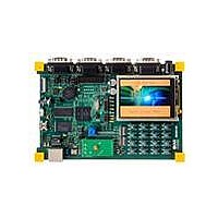
Manufacturer Part Number
IAR-KSK-IMX25
Description
KIT DEVELOPMENT I.MX257, ARM926
Manufacturer
Freescale Semiconductor
Series
i.MX25r
Type
MCUr
Datasheets
1.MCIMX25WPDKJ.pdf
(2 pages)
2.IAR-KSK-IMX25.pdf
(154 pages)
3.IAR-KSK-IMX25.pdf
(2 pages)
4.IAR-KSK-IMX25.pdf
(57 pages)
Specifications of IAR-KSK-IMX25
Contents
Board, Cables, CD, Debugger, Power Supply
Processor To Be Evaluated
I.MX257
Processor Series
i.MX25
Data Bus Width
16 bit
Interface Type
UART, JTAG, USB, Ethernet, SD/MMC
Core
ARM926EJ-S
Silicon Manufacturer
Freescale
Core Architecture
ARM
Core Sub-architecture
ARM9
Silicon Core Number
I.MX2
Silicon Family Name
I.MX25
Mcu Supported Families
I.MX25
For Use With/related Products
i.MX25
Lead Free Status / RoHS Status
Lead free / RoHS Compliant


1.Maximum condition for tpr, tpo, and tpv: wcs model, 1.1 V, IO 3.0 V and 105 °C. Minimum condition for tpr, tpo, and tpv: bcs
2. Minimum condition for tps: wcs model, 1.1 V, IO 3.0 V and 105 °C. tps is measured between VIL to VIH for rising edge and
3. Maximum condition for tdit: bcs model, 1.3 V, IO 3.6 V and –40 °C.
4. Maximum condition for tpi and trfi: wcs model, 1.1 V, IO 3.0 V and 105 °C. Minimum condition for tpi and trfi: bcs model, 1.3 V,
5. Hysteresis mode is recommended for input with transition time greater than 25 ns.
3.6.3
The DDR pad type is configured by the IOMUXC_SW_PAD_CTL_GRP_DDRTYPE register (see
Chapter 4, “External Signals and Pin Multiplexing,” in the i.MX25 Multimedia Applications Processor
Reference Manual).
3.6.3.1
Table 24
1.8V (± 5%) applications.
Freescale Semiconductor
Input Pad Propagation Delay without
Hysteresis, 50%–50%
Input Pad Propagation Delay with Hysteresis,
50%–50%
Input Pad Propagation Delay without
Hysteresis, 40%–60%
Input Pad Propagation Delay with Hysteresis,
40%–60%
Input Pad Transition Times without Hysteresis
Input Pad Transition Times with Hysteresis
Maximum Input Transition Times
Duty cycle
Clock frequency
Output pad transition times (max. drive)
Output pad transition times (high drive)
Output pad transition times (standard drive)
model, 1.3 V, IO 3.6 V and –40 °C. Input transition time from core is 1ns (20%–80%).
between VIH to VIL for falling edge.
IO 3.6 V and –40 °C. Input transition time from pad is 5ns (20%–80%).
shows AC parameters for mobile DDR I/O. These settings are suitable for mDDR and DDR2
DDR I/O AC Parameters
DDR_TYPE = 00 Standard Setting I/O AC Parameters and Requirements
Parameter
i.MX25 Applications Processor for Consumer and Industrial Products, Rev. 8
Table 23. Fast I/O AC Parameters for OVDD = 3.0
Table 24. AC Parameters for Mobile DDR I/O
Symbol
Fduty
tpr
tpr
tpr
trm
trfi
trfi
f
tpi
tpi
tpi
tpi
Condition
1.6pF
1.6pF
1.6pF
1.6pF
1.6pF
1.6pF
25 pF
50 pF
25 pF
50 pF
25 pF
50 pF
—
Load
—
—
0.729/0.458 0.97/0.0649 1.404/0.97
1.203/0.938 1.172/1.187 1.713/1.535
0.879/0.977 1.434/1.12 1.854/1.427
1.353/1.457 1.637/1.659 2.163/1.991
0.16/0.12
0.16/0.13
Rise/Fall
0.52/0.51
0.98/0.96
1.13/1.10
2.15/2.10
2.26/2.19
4.30/4.18
—
Min.
40
—
–
3.6 V (continued)
0.23/0.18
0.22/0.18
0.79/0.72
1.49/1.34
1.74/1.55
3.28/2.92
3.46/3.07
6.59/5.79
Typ.
—
50
—
10.13/8.55
Rise/Fall
1.25/1.09
2.31/1.98
2.71/2.30
5.11/4.31
5.39/4.56
0.33/0.29
0.33/0.29
Max.
133
60
—
Units
MHz
ns
ns
ns
%
ns
ns
ns
ns
ns
ns
ns
Notes
—
1
1
4
5
33
Related parts for IAR-KSK-IMX25
Image
Part Number
Description
Manufacturer
Datasheet
Request
R

Part Number:
Description:
Manufacturer:
Freescale Semiconductor, Inc
Datasheet:
Part Number:
Description:
Manufacturer:
Freescale Semiconductor, Inc
Datasheet:
Part Number:
Description:
Manufacturer:
Freescale Semiconductor, Inc
Datasheet:
Part Number:
Description:
Manufacturer:
Freescale Semiconductor, Inc
Datasheet:
Part Number:
Description:
Manufacturer:
Freescale Semiconductor, Inc
Datasheet:
Part Number:
Description:
Manufacturer:
Freescale Semiconductor, Inc
Datasheet:
Part Number:
Description:
Manufacturer:
Freescale Semiconductor, Inc
Datasheet:
Part Number:
Description:
Manufacturer:
Freescale Semiconductor, Inc
Datasheet:
Part Number:
Description:
Manufacturer:
Freescale Semiconductor, Inc
Datasheet:
Part Number:
Description:
Manufacturer:
Freescale Semiconductor, Inc
Datasheet:
Part Number:
Description:
Manufacturer:
Freescale Semiconductor, Inc
Datasheet:
Part Number:
Description:
Manufacturer:
Freescale Semiconductor, Inc
Datasheet:
Part Number:
Description:
Manufacturer:
Freescale Semiconductor, Inc
Datasheet:
Part Number:
Description:
Manufacturer:
Freescale Semiconductor, Inc
Datasheet:
Part Number:
Description:
Manufacturer:
Freescale Semiconductor, Inc
Datasheet: