IAR-KSK-IMX25 Freescale Semiconductor, IAR-KSK-IMX25 Datasheet - Page 48
IAR-KSK-IMX25
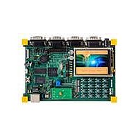
Manufacturer Part Number
IAR-KSK-IMX25
Description
KIT DEVELOPMENT I.MX257, ARM926
Manufacturer
Freescale Semiconductor
Series
i.MX25r
Type
MCUr
Datasheets
1.MCIMX25WPDKJ.pdf
(2 pages)
2.IAR-KSK-IMX25.pdf
(154 pages)
3.IAR-KSK-IMX25.pdf
(2 pages)
4.IAR-KSK-IMX25.pdf
(57 pages)
Specifications of IAR-KSK-IMX25
Contents
Board, Cables, CD, Debugger, Power Supply
Processor To Be Evaluated
I.MX257
Processor Series
i.MX25
Data Bus Width
16 bit
Interface Type
UART, JTAG, USB, Ethernet, SD/MMC
Core
ARM926EJ-S
Silicon Manufacturer
Freescale
Core Architecture
ARM
Core Sub-architecture
ARM9
Silicon Core Number
I.MX2
Silicon Family Name
I.MX25
Mcu Supported Families
I.MX25
For Use With/related Products
i.MX25
Lead Free Status / RoHS Status
Lead free / RoHS Compliant


To meet timing requirements, a number of timing parameters must be controlled. See
on timing parameters for MDMA read and write modes.
1
2
3
3.7.2.3
UDMA mode timing is more complicated than PIO mode or MDMA mode. In this section, timing
diagrams for UDMA in- and out-transfers are provided.
48
Parameter
tg(write)
See
See
tk1 in the UDMA figures equals (tk –2 × T).
tg(read)
tf(write)
tf(read)
tm, ti
ATA
tn, tj
—
td
tk
t0
tL
Figure
Figure
MDMA Read
13.
14.
Parameters
and Write
Ultra DMA (UDMA) Mode Timing
Timing
td, td1
tkjn
ton
toff
tgr
tm
—
—
—
tfr
—
tk
i.MX25 Applications Processor for Consumer and Industrial Products, Rev. 8
2
Table 38. Timing Parameters for MDMA Read and Write Modes
1
Write Data(15:0)
tm(min.) = ti(min.) = time_m × T – (tskew1 + tskew2 + tskew5)
td1(min.) = td(min.) = time_d × T – (tskew1 + tskew2 + tskew6)
tk(min.) = time_k × T – (tskew1 + tskew2 + tskew6)
t0(min.) = (time_d + time_k) × T
tgr(min.–read) = tco + tsu + tbuf + tbuf + tcable1 + tcable2
tgr(min.–drive) = td – te(drive)
tfr(min.–drive) =0 k
tg(min.–write) = time_d × T –(tskew1 + tskew2 + tskew5)
tf(min.–write) = time_k × T – (tskew1 + tskew2 + tskew6)
tL(max.) = (time_d + time_k–2) × T – (tsu + tco + 2 × tbuf + 2 × tcable2)
tn= tj= tkjn = (max.(time_k,. time_jn) × T – (tskew1 + tskew2 + tskew6)
ton = time_on × T – tskew1
toff = time_off × T – tskew1
ADDR
(See note 1)
buffer_en
DMACK
DMARQ
DIOW
Figure 14. MDMA Write Mode Timing
tm ton td1
Relation
tk
td
tk1
tkjn
toff
Freescale Semiconductor
Table 38
time_d, time_k
time_d, time_k
Parameter(s)
Adjustable
time_m
time_jn
time_d
time_k
time_d
time_d
time_k
—
—
for details
3
Related parts for IAR-KSK-IMX25
Image
Part Number
Description
Manufacturer
Datasheet
Request
R

Part Number:
Description:
Manufacturer:
Freescale Semiconductor, Inc
Datasheet:
Part Number:
Description:
Manufacturer:
Freescale Semiconductor, Inc
Datasheet:
Part Number:
Description:
Manufacturer:
Freescale Semiconductor, Inc
Datasheet:
Part Number:
Description:
Manufacturer:
Freescale Semiconductor, Inc
Datasheet:
Part Number:
Description:
Manufacturer:
Freescale Semiconductor, Inc
Datasheet:
Part Number:
Description:
Manufacturer:
Freescale Semiconductor, Inc
Datasheet:
Part Number:
Description:
Manufacturer:
Freescale Semiconductor, Inc
Datasheet:
Part Number:
Description:
Manufacturer:
Freescale Semiconductor, Inc
Datasheet:
Part Number:
Description:
Manufacturer:
Freescale Semiconductor, Inc
Datasheet:
Part Number:
Description:
Manufacturer:
Freescale Semiconductor, Inc
Datasheet:
Part Number:
Description:
Manufacturer:
Freescale Semiconductor, Inc
Datasheet:
Part Number:
Description:
Manufacturer:
Freescale Semiconductor, Inc
Datasheet:
Part Number:
Description:
Manufacturer:
Freescale Semiconductor, Inc
Datasheet:
Part Number:
Description:
Manufacturer:
Freescale Semiconductor, Inc
Datasheet:
Part Number:
Description:
Manufacturer:
Freescale Semiconductor, Inc
Datasheet: