IAR-KSK-IMX25 Freescale Semiconductor, IAR-KSK-IMX25 Datasheet - Page 36
IAR-KSK-IMX25
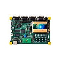
Manufacturer Part Number
IAR-KSK-IMX25
Description
KIT DEVELOPMENT I.MX257, ARM926
Manufacturer
Freescale Semiconductor
Series
i.MX25r
Type
MCUr
Datasheets
1.MCIMX25WPDKJ.pdf
(2 pages)
2.IAR-KSK-IMX25.pdf
(154 pages)
3.IAR-KSK-IMX25.pdf
(2 pages)
4.IAR-KSK-IMX25.pdf
(57 pages)
Specifications of IAR-KSK-IMX25
Contents
Board, Cables, CD, Debugger, Power Supply
Processor To Be Evaluated
I.MX257
Processor Series
i.MX25
Data Bus Width
16 bit
Interface Type
UART, JTAG, USB, Ethernet, SD/MMC
Core
ARM926EJ-S
Silicon Manufacturer
Freescale
Core Architecture
ARM
Core Sub-architecture
ARM9
Silicon Core Number
I.MX2
Silicon Family Name
I.MX25
Mcu Supported Families
I.MX25
For Use With/related Products
i.MX25
Lead Free Status / RoHS Status
Lead free / RoHS Compliant


Note:
1. Maximum condition for tpr, tpo, tpi, and tpv: wcs model, 1.1 V, I/O 1.65 V, and 105 °C. Minimum condition for tpr, tpo, and tpv:
2. Minimum condition for tps: wcs model, 1.1 V, I/O 1.65 V, and 105 °C. tps is measured between VIL to VIH for rising edge and
3. Maximum condition for tdit: bcs model, 1.3 V, I/O 1.95 V, and –40 °C.
4. Maximum condition for tpi and trfi: wcs model, 1.1 V, I/O 1.65 V and 105 °C. Minimum condition for tpi and trfi: bcs model, 1.3 V,
Table 26
36
Output enable to output valid delay (max.
drive), 40%–60%
Output enable to output valid delay (high
drive), 40%–60%
Output enable to output valid delay
(standard drive), 40%–60%
Output pad slew rate (max. drive)
Output pad slew rate (high drive)
Output pad slew rate (standard drive)
Output pad dI/dt (max. drive)
Output pad dI/dt (high drive)
Output pad dI/dt (standard drive)
Input pad transition times
Input pad propagation delay, 50%–50%
Input pad propagation delay, 40%–60%
AC input logic high
AC input logic low
AC differential input voltage
AC differential cross point voltage for input
bcs model, 1.3 V, I/O 1.95 V and –40 °C. Input transition time from core is 1 ns (20%–80%).
between VIH to VIL for falling edge.
I/O 1.95 V and –40 °C. Input transition time from pad is 5 ns (20%–80%).
shows the AC requirements for mobile DDR I/O.
Parameter
Table 25. AC Parameters for Mobile DDR pbijtov18_33_ddr_clk I/O (continued)
Parameter
i.MX25 Applications Processor for Consumer and Industrial Products, Rev. 8
Table 26. AC Requirements for Mobile DDR I/O
Symbol
tps
tps
tps
tdit
tdit
tdit
tpv
tpv
tpv
trfi
tpi
tpi
Symbol
VIH(ac)
VIL(ac)
Vid(ac)
Vix(ac)
Condition
1.0 pF
1.0 pF
1.0 pF
15 pF
35 pF
15 pF
35 pF
15 pF
35 pF
25 pF
50 pF
25 pF
50 pF
25 pF
50 pF
25 pF
50 pF
25 pF
50 pF
25 pF
50 pF
Load
0.4 × OVDD
0.8 × OVDD
0.6 × OVDD
Rise/Fall
1.28/1.24
1.49/1.47
1.45/1.44
1.92/1.95
1.85/1.88
2.78/2.88
0.37/0.45
0.30/0.36
0.30/0.37
0.21/0.25
0.22/0.26
0.13/0.16
0.07/0.08
0.84/0.84
1.66/1.66
Min.
–0.3
Min.
65
70
31
33
16
17
2.00/1.90
2.32/2.21
2.28/2.19
2.99/2.87
2.92/2.79
4.34/4.16
0.64/0.79
0.52/0.61
0.51/0.63
0.36/0.42
0.37/0.44
0.23/0.26
0.11/0.13
1.40/1.34
2.22/2.16
Typ.
171
183
82
87
43
46
0.2 × OVDD
OVDD+0.3
OVDD+0.6
OVDD+0.6
4.5894.25
3.14/2.93
3.64/3.41
3.60/3.36
4.69/4.36
6.79/6.24
1.14/1.36
0.90/1.02
0.63/0.67
0.65/0.72
0.39/0.40
0.16/0.20
2.25/2.16
3.06/2.97
Rise/Fall
091/1.06
Max.
Max.
426
450
233
245
115
120
Freescale Semiconductor
mA/ns
mA/ns
mA/ns
Units
V/ns
V/ns
V/ns
ns
ns
ns
ns
ns
ns
Units
Notes
V
V
V
V
1
2
3
4
Related parts for IAR-KSK-IMX25
Image
Part Number
Description
Manufacturer
Datasheet
Request
R

Part Number:
Description:
Manufacturer:
Freescale Semiconductor, Inc
Datasheet:
Part Number:
Description:
Manufacturer:
Freescale Semiconductor, Inc
Datasheet:
Part Number:
Description:
Manufacturer:
Freescale Semiconductor, Inc
Datasheet:
Part Number:
Description:
Manufacturer:
Freescale Semiconductor, Inc
Datasheet:
Part Number:
Description:
Manufacturer:
Freescale Semiconductor, Inc
Datasheet:
Part Number:
Description:
Manufacturer:
Freescale Semiconductor, Inc
Datasheet:
Part Number:
Description:
Manufacturer:
Freescale Semiconductor, Inc
Datasheet:
Part Number:
Description:
Manufacturer:
Freescale Semiconductor, Inc
Datasheet:
Part Number:
Description:
Manufacturer:
Freescale Semiconductor, Inc
Datasheet:
Part Number:
Description:
Manufacturer:
Freescale Semiconductor, Inc
Datasheet:
Part Number:
Description:
Manufacturer:
Freescale Semiconductor, Inc
Datasheet:
Part Number:
Description:
Manufacturer:
Freescale Semiconductor, Inc
Datasheet:
Part Number:
Description:
Manufacturer:
Freescale Semiconductor, Inc
Datasheet:
Part Number:
Description:
Manufacturer:
Freescale Semiconductor, Inc
Datasheet:
Part Number:
Description:
Manufacturer:
Freescale Semiconductor, Inc
Datasheet: