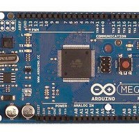
A000047 Arduino, A000047 Datasheet - Page 115
A000047
Manufacturer Part Number
A000047
Description
MCU, MPU & DSP Development Tools Mega2560
Manufacturer
Arduino
Series
-r
Type
MCUr
Specifications of A000047
Processor To Be Evaluated
ATmega2560
Interface Type
USB, I2C, SPI
Dimensions
4 in x 2.1 in
Operating Supply Voltage
5 V
Contents
Board
Lead Free Status / RoHS Status
Lead free / RoHS Compliant
For Use With/related Products
ATmega2560


14.2.3
14.2.4
14.2.5
2549M–AVR–09/10
EIMSK – External Interrupt Mask Register
EIFR – External Interrupt Flag Register
PCICR – Pin Change Interrupt Control Register
• Bits 7:0 – INT7:0: External Interrupt Request 7 - 0 Enable
When an INT7:0 bit is written to one and the I-bit in the Status Register (SREG) is set (one), the
corresponding external pin interrupt is enabled. The Interrupt Sense Control bits in the External
Interrupt Control Registers – EICRA and EICRB – defines whether the external interrupt is acti-
vated on rising or falling edge or level sensed. Activity on any of these pins will trigger an
interrupt request even if the pin is enabled as an output. This provides a way of generating a
software interrupt.
• Bits 7:0 – INTF7:0: External Interrupt Flags 7 - 0
When an edge or logic change on the INT7:0 pin triggers an interrupt request, INTF7:0 becomes
set (one). If the I-bit in SREG and the corresponding interrupt enable bit, INT7:0 in EIMSK, are
set (one), the MCU will jump to the interrupt vector. The flag is cleared when the interrupt routine
is executed. Alternatively, the flag can be cleared by writing a logical one to it. These flags are
always cleared when INT7:0 are configured as level interrupt. Note that when entering sleep
mode with the INT3:0 interrupts disabled, the input buffers on these pins will be disabled. This
may cause a logic change in internal signals which will set the INTF3:0 flags. See
Enable and Sleep Modes” on page 74
• Bit 2 – PCIE2: Pin Change Interrupt Enable 1
When the PCIE2 bit is set (one) and the I-bit in the Status Register (SREG) is set (one), pin
change interrupt 2 is enabled. Any change on any enabled PCINT23:16 pin will cause an inter-
rupt. The corresponding interrupt of Pin Change Interrupt Request is executed from the PCI2
Interrupt Vector. PCINT23:16 pins are enabled individually by the PCMSK2 Register.
• Bit 1 – PCIE1: Pin Change Interrupt Enable 1
When the PCIE1 bit is set (one) and the I-bit in the Status Register (SREG) is set (one), pin
change interrupt 1 is enabled. Any change on any enabled PCINT15:8 pin will cause an inter-
rupt. The corresponding interrupt of Pin Change Interrupt Request is executed from the PCI1
Interrupt Vector. PCINT15:8 pins are enabled individually by the PCMSK1 Register.
Bit
0x1D (0x3D)
Read/Write
Initial Value
Bit
0x1C (0x3C)
Read/Write
Initial Value
Bit
(0x68)
Read/Write
Initial Value
INTF7
INT7
R/W
R/W
7
0
7
0
R
7
–
0
INTF6
INT6
R/W
R/W
6
0
6
0
R
6
–
0
ATmega640/1280/1281/2560/2561
INTF5
INT5
R/W
R/W
5
0
5
0
R
5
–
0
for more information.
INTF4
INT4
R/W
R/W
4
0
4
0
R
4
–
0
INTF3
INT3
R/W
R/W
3
0
3
0
R
3
–
0
INTF2
INT2
PCIE2
R/W
R/W
R/W
2
0
2
0
2
0
INTF1
INT1
PCIE1
R/W
R/W
R/W
1
0
1
0
1
0
IINTF0
INT0
R/W
R/W
PCIE0
R/W
0
0
0
0
0
0
“Digital Input
EIMSK
PCICR
EIFR
115
Related parts for A000047
Image
Part Number
Description
Manufacturer
Datasheet
Request
R

Part Number:
Description:
Daughter Cards & OEM Boards ARDUINO UNO PROTO PCB REV 3
Manufacturer:
Arduino
Part Number:
Description:
Daughter Cards & OEM Boards ARDUINO SHIELD PROTO KIT REV 3
Manufacturer:
Arduino
Part Number:
Description:
Daughter Cards & OEM Boards ARDUINO MEGA PROTO KIT REV 3
Manufacturer:
Arduino
Part Number:
Description:
Daughter Cards & OEM Boards ARDUINO MEGA PROTO PCB REV 3
Manufacturer:
Arduino
Part Number:
Description:
Development Boards & Kits - AVR ARDUINO STARTER KIT W/ UNO REV3
Manufacturer:
Arduino
Part Number:
Description:
RF Development Tools ARDUINO SHIELD WIRELESS PROTO
Manufacturer:
Arduino
Datasheet:
Part Number:
Description:
RF Development Tools ARDUINO SHIELD WIRELESS WITH SD
Manufacturer:
Arduino
Datasheet:

Part Number:
Description:
Development Software Getting started w/Arduino
Manufacturer:
Arduino

Part Number:
Description:
Ethernet Modules & Development Tools Ethernet Shield for Arduino
Manufacturer:
Arduino

Part Number:
Description:
MCU, MPU & DSP Development Tools LilyPad Arduino Main Board
Manufacturer:
Arduino

Part Number:
Description:
ARDUINO NANO Board
Manufacturer:
Arduino
Datasheet:
Part Number:
Description:
Ethernet Modules & Development Tools ETHERNET SHEILD PoE FOR ARDUINO
Manufacturer:
Arduino
Datasheet:

Part Number:
Description:
ATMEGA328 MCU IC W/ Arduino UNO Bootloader
Manufacturer:
Arduino
Datasheet:
Part Number:
Description:
Memory Cards MICRO SD CARD 1GB WITH SD ADAPTER
Manufacturer:
Arduino