A000047 Arduino, A000047 Datasheet - Page 32
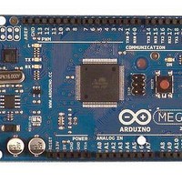
A000047
Manufacturer Part Number
A000047
Description
MCU, MPU & DSP Development Tools Mega2560
Manufacturer
Arduino
Series
-r
Type
MCUr
Specifications of A000047
Processor To Be Evaluated
ATmega2560
Interface Type
USB, I2C, SPI
Dimensions
4 in x 2.1 in
Operating Supply Voltage
5 V
Contents
Board
Lead Free Status / RoHS Status
Lead free / RoHS Compliant
For Use With/related Products
ATmega2560


8.1.5
2549M–AVR–09/10
Using all Locations of External Memory Smaller than 64 Kbytes
Figure 8-5.
Note:
Figure 8-6.
Note:
Since the external memory is mapped after the internal memory as shown in
28, the external memory is not addressed when addressing the first 8,704 bytes of data space. It
may appear that the first 8,704 bytes of the external memory are inaccessible (external memory
addresses 0x0000 to 0x21FF). However, when connecting an external memory smaller than 64
Kbytes, for example 32 Kbytes, these locations are easily accessed simply by addressing from
address 0x8000 to 0xA1FF. Since the External Memory Address bit A15 is not connected to the
external memory, addresses 0x8000 to 0xA1FF will appear as addresses 0x0000 to 0x21FF for
the external memory. Addressing above address 0xA1FF is not recommended, since this will
address an external memory location that is already accessed by another (lower) address. To
System Clock (CLK
System Clock (CLK
DA7:0 (XMBK = 0)
DA7:0 (XMBK = 1)
DA7:0 (XMBK = 0)
DA7:0 (XMBK = 1)
1. SRWn1 = SRW11 (upper sector) or SRW01 (lower sector), SRWn0 = SRW10 (upper sector) or
1. SRWn1 = SRW11 (upper sector) or SRW01 (lower sector), SRWn0 = SRW10 (upper sector) or
SRW00 (lower sector).
The ALE pulse in period T6 is only present if the next instruction accesses the RAM (internal
or external).
SRW00 (lower sector).
The ALE pulse in period T7 is only present if the next instruction accesses the RAM (internal
or external).
DA7:0
A15:8
CPU
ALE
DA7:0
WR
A15:8
RD
External Data Memory Cycles with SRWn1 = 1 and SRWn0 = 0
External Data Memory Cycles with SRWn1 = 1 and SRWn0 = 1
CPU
ALE
WR
)
RD
)
Prev. addr.
Prev. data
Prev. data
Prev. data
Prev. addr.
Prev. data
Prev. data
Prev. data
T1
T1
Address
Address
Address
ATmega640/1280/1281/2560/2561
T2
Address
Address
Address
XX
T2
XX
Address
T3
Data
Data
Data
Address
T3
Data
Data
Data
T4
T4
T5
T5
T6
Figure 8-1 on page
(1)
(1)
T6
T7
32
Related parts for A000047
Image
Part Number
Description
Manufacturer
Datasheet
Request
R

Part Number:
Description:
Daughter Cards & OEM Boards ARDUINO UNO PROTO PCB REV 3
Manufacturer:
Arduino
Part Number:
Description:
Daughter Cards & OEM Boards ARDUINO SHIELD PROTO KIT REV 3
Manufacturer:
Arduino
Part Number:
Description:
Daughter Cards & OEM Boards ARDUINO MEGA PROTO KIT REV 3
Manufacturer:
Arduino
Part Number:
Description:
Daughter Cards & OEM Boards ARDUINO MEGA PROTO PCB REV 3
Manufacturer:
Arduino
Part Number:
Description:
Development Boards & Kits - AVR ARDUINO STARTER KIT W/ UNO REV3
Manufacturer:
Arduino
Part Number:
Description:
RF Development Tools ARDUINO SHIELD WIRELESS PROTO
Manufacturer:
Arduino
Datasheet:
Part Number:
Description:
RF Development Tools ARDUINO SHIELD WIRELESS WITH SD
Manufacturer:
Arduino
Datasheet:

Part Number:
Description:
Development Software Getting started w/Arduino
Manufacturer:
Arduino

Part Number:
Description:
Ethernet Modules & Development Tools Ethernet Shield for Arduino
Manufacturer:
Arduino

Part Number:
Description:
MCU, MPU & DSP Development Tools LilyPad Arduino Main Board
Manufacturer:
Arduino

Part Number:
Description:
ARDUINO NANO Board
Manufacturer:
Arduino
Datasheet:
Part Number:
Description:
Ethernet Modules & Development Tools ETHERNET SHEILD PoE FOR ARDUINO
Manufacturer:
Arduino
Datasheet:

Part Number:
Description:
ATMEGA328 MCU IC W/ Arduino UNO Bootloader
Manufacturer:
Arduino
Datasheet:
Part Number:
Description:
Memory Cards MICRO SD CARD 1GB WITH SD ADAPTER
Manufacturer:
Arduino