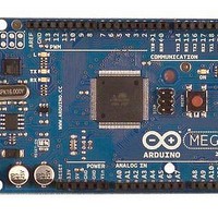
A000047 Arduino, A000047 Datasheet - Page 153
A000047
Manufacturer Part Number
A000047
Description
MCU, MPU & DSP Development Tools Mega2560
Manufacturer
Arduino
Series
-r
Type
MCUr
Specifications of A000047
Processor To Be Evaluated
ATmega2560
Interface Type
USB, I2C, SPI
Dimensions
4 in x 2.1 in
Operating Supply Voltage
5 V
Contents
Board
Lead Free Status / RoHS Status
Lead free / RoHS Compliant
For Use With/related Products
ATmega2560


2549M–AVR–09/10
Figure 16-8. Phase Correct PWM Mode, Timing Diagram
The Timer/Counter Overflow Flag (TOVn) is set each time the counter reaches BOTTOM. When
either OCRnA or ICRn is used for defining the TOP value, the OCnA or ICFn Flag is set accord-
ingly at the same timer clock cycle as the OCRnx Registers are updated with the double buffer
value (at TOP). The Interrupt Flags can be used to generate an interrupt each time the counter
reaches the TOP or BOTTOM value.
When changing the TOP value the program must ensure that the new TOP value is higher or
equal to the value of all of the Compare Registers. If the TOP value is lower than any of the
Compare Registers, a compare match will never occur between the TCNTn and the OCRnx.
Note that when using fixed TOP values, the unused bits are masked to zero when any of the
OCRnx Registers are written. As the third period shown in
TOP actively while the Timer/Counter is running in the phase correct mode can result in an
unsymmetrical output. The reason for this can be found in the time of update of the OCRnx Reg-
ister. Since the OCRnx update occurs at TOP, the PWM period starts and ends at TOP. This
implies that the length of the falling slope is determined by the previous TOP value, while the
length of the rising slope is determined by the new TOP value. When these two values differ the
two slopes of the period will differ in length. The difference in length gives the unsymmetrical
result on the output.
It is recommended to use the phase and frequency correct mode instead of the phase correct
mode when changing the TOP value while the Timer/Counter is running. When using a static
TOP value there are practically no differences between the two modes of operation.
In phase correct PWM mode, the compare units allow generation of PWM waveforms on the
OCnx pins. Setting the COMnx1:0 bits to two will produce a non-inverted PWM and an inverted
PWM output can be generated by setting the COMnx1:0 to three (see
The actual OCnx value will only be visible on the port pin if the data direction for the port pin is
set as output (DDR_OCnx). The PWM waveform is generated by setting (or clearing) the OCnx
Register at the compare match between OCRnx and TCNTn when the counter increments, and
clearing (or setting) the OCnx Register at compare match between OCRnx and TCNTn when
TCNTn
OCnx
OCnx
Period
1
ATmega640/1280/1281/2560/2561
2
3
Figure 16-8
4
Table 16-5 on page
illustrates, changing the
OCRnx/TOP Update and
OCnA Interrupt Flag Set
or ICFn Interrupt Flag Set
(Interrupt on TOP)
TOVn Interrupt Flag Set
(Interrupt on Bottom)
(COMnx1:0 = 2)
(COMnx1:0 = 3)
160).
153
Related parts for A000047
Image
Part Number
Description
Manufacturer
Datasheet
Request
R

Part Number:
Description:
Daughter Cards & OEM Boards ARDUINO UNO PROTO PCB REV 3
Manufacturer:
Arduino
Part Number:
Description:
Daughter Cards & OEM Boards ARDUINO SHIELD PROTO KIT REV 3
Manufacturer:
Arduino
Part Number:
Description:
Daughter Cards & OEM Boards ARDUINO MEGA PROTO KIT REV 3
Manufacturer:
Arduino
Part Number:
Description:
Daughter Cards & OEM Boards ARDUINO MEGA PROTO PCB REV 3
Manufacturer:
Arduino
Part Number:
Description:
Development Boards & Kits - AVR ARDUINO STARTER KIT W/ UNO REV3
Manufacturer:
Arduino
Part Number:
Description:
RF Development Tools ARDUINO SHIELD WIRELESS PROTO
Manufacturer:
Arduino
Datasheet:
Part Number:
Description:
RF Development Tools ARDUINO SHIELD WIRELESS WITH SD
Manufacturer:
Arduino
Datasheet:

Part Number:
Description:
Development Software Getting started w/Arduino
Manufacturer:
Arduino

Part Number:
Description:
Ethernet Modules & Development Tools Ethernet Shield for Arduino
Manufacturer:
Arduino

Part Number:
Description:
MCU, MPU & DSP Development Tools LilyPad Arduino Main Board
Manufacturer:
Arduino

Part Number:
Description:
ARDUINO NANO Board
Manufacturer:
Arduino
Datasheet:
Part Number:
Description:
Ethernet Modules & Development Tools ETHERNET SHEILD PoE FOR ARDUINO
Manufacturer:
Arduino
Datasheet:

Part Number:
Description:
ATMEGA328 MCU IC W/ Arduino UNO Bootloader
Manufacturer:
Arduino
Datasheet:
Part Number:
Description:
Memory Cards MICRO SD CARD 1GB WITH SD ADAPTER
Manufacturer:
Arduino