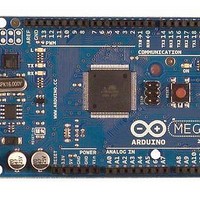
A000047 Arduino, A000047 Datasheet - Page 206
A000047
Manufacturer Part Number
A000047
Description
MCU, MPU & DSP Development Tools Mega2560
Manufacturer
Arduino
Series
-r
Type
MCUr
Specifications of A000047
Processor To Be Evaluated
ATmega2560
Interface Type
USB, I2C, SPI
Dimensions
4 in x 2.1 in
Operating Supply Voltage
5 V
Contents
Board
Lead Free Status / RoHS Status
Lead free / RoHS Compliant
For Use With/related Products
ATmega2560


21.2
2549M–AVR–09/10
Clock Generation
Figure 21-1. USART Block Diagram
Note:
The dashed boxes in the block diagram separate the three main parts of the USART (listed from
the top): Clock Generator, Transmitter and Receiver. Control Registers are shared by all units.
The Clock Generation logic consists of synchronization logic for external clock input used by
synchronous slave operation, and the baud rate generator. The XCKn (Transfer Clock) pin is
only used by synchronous transfer mode. The Transmitter consists of a single write buffer, a
serial Shift Register, Parity Generator and Control logic for handling different serial frame for-
mats. The write buffer allows a continuous transfer of data without any delay between frames.
The Receiver is the most complex part of the USART module due to its clock and data recovery
units. The recovery units are used for asynchronous data reception. In addition to the recovery
units, the Receiver includes a Parity Checker, Control logic, a Shift Register and a two level
receive buffer (UDRn). The Receiver supports the same frame formats as the Transmitter, and
can detect Frame Error, Data OverRun and Parity Errors.
The Clock Generation logic generates the base clock for the Transmitter and Receiver. The
USARTn supports four modes of clock operation: Normal asynchronous, Double Speed asyn-
chronous, Master synchronous and Slave synchronous mode. The UMSELn bit in USART
Control and Status Register C (UCSRnC) selects between asynchronous and synchronous
operation. Double Speed (asynchronous mode only) is controlled by the U2Xn found in the
1. See
page
Figure 1-1 on page
86,
Table 12-24 on page 92
UCSRA
TRANSMIT SHIFT REGISTER
RECEIVE SHIFT REGISTER
BAUD RATE GENERATOR
ATmega640/1280/1281/2560/2561
2,
UDR (Transmit)
UDR (Receive)
UBRR[H:L]
Figure 1-3 on page
(1)
and
Table 12-27 on page 94
UCSRB
GENERATOR
SYNC LOGIC
RECOVERY
RECOVERY
4,
CHECKER
PARITY
CLOCK
PARITY
DATA
OSC
Table 12-12 on page
Clock Generator
for USART pin placement.
CONTROL
CONTROL
CONTROL
CONTROL
CONTROL
Transmitter
PIN
PIN
PIN
TX
RX
Receiver
UCSRC
83,
Table 12-15 on
XCK
RxD
TxD
206
Related parts for A000047
Image
Part Number
Description
Manufacturer
Datasheet
Request
R

Part Number:
Description:
Daughter Cards & OEM Boards ARDUINO UNO PROTO PCB REV 3
Manufacturer:
Arduino
Part Number:
Description:
Daughter Cards & OEM Boards ARDUINO SHIELD PROTO KIT REV 3
Manufacturer:
Arduino
Part Number:
Description:
Daughter Cards & OEM Boards ARDUINO MEGA PROTO KIT REV 3
Manufacturer:
Arduino
Part Number:
Description:
Daughter Cards & OEM Boards ARDUINO MEGA PROTO PCB REV 3
Manufacturer:
Arduino
Part Number:
Description:
Development Boards & Kits - AVR ARDUINO STARTER KIT W/ UNO REV3
Manufacturer:
Arduino
Part Number:
Description:
RF Development Tools ARDUINO SHIELD WIRELESS PROTO
Manufacturer:
Arduino
Datasheet:
Part Number:
Description:
RF Development Tools ARDUINO SHIELD WIRELESS WITH SD
Manufacturer:
Arduino
Datasheet:

Part Number:
Description:
Development Software Getting started w/Arduino
Manufacturer:
Arduino

Part Number:
Description:
Ethernet Modules & Development Tools Ethernet Shield for Arduino
Manufacturer:
Arduino

Part Number:
Description:
MCU, MPU & DSP Development Tools LilyPad Arduino Main Board
Manufacturer:
Arduino

Part Number:
Description:
ARDUINO NANO Board
Manufacturer:
Arduino
Datasheet:
Part Number:
Description:
Ethernet Modules & Development Tools ETHERNET SHEILD PoE FOR ARDUINO
Manufacturer:
Arduino
Datasheet:

Part Number:
Description:
ATMEGA328 MCU IC W/ Arduino UNO Bootloader
Manufacturer:
Arduino
Datasheet:
Part Number:
Description:
Memory Cards MICRO SD CARD 1GB WITH SD ADAPTER
Manufacturer:
Arduino