A000047 Arduino, A000047 Datasheet - Page 275
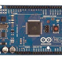
A000047
Manufacturer Part Number
A000047
Description
MCU, MPU & DSP Development Tools Mega2560
Manufacturer
Arduino
Series
-r
Type
MCUr
Specifications of A000047
Processor To Be Evaluated
ATmega2560
Interface Type
USB, I2C, SPI
Dimensions
4 in x 2.1 in
Operating Supply Voltage
5 V
Contents
Board
Lead Free Status / RoHS Status
Lead free / RoHS Compliant
For Use With/related Products
ATmega2560


25. ADC – Analog to Digital Converter
25.1
2549M–AVR–09/10
Features
•
•
•
•
•
•
•
•
•
•
•
•
•
•
•
The ATmega640/1280/1281/2560/2561 features a 10-bit successive approximation ADC. The
ADC is connected to an 8/16-channel Analog Multiplexer which allows eight/sixteen single-
ended voltage inputs constructed from the pins of Port F and Port K. The single-ended voltage
inputs refer to 0V (GND).
The device also supports 16/32 differential voltage input combinations. Four of the differential
inputs (ADC1 & ADC0, ADC3 & ADC2, ADC9 & ADC8 and ADC11 & ADC10) are equipped with
a programmable gain stage, providing amplification steps of 0 dB (1×), 20 dB (10×) or 46 dB
(200×) on the differential input voltage before the ADC conversion. The 16 channels are split in
two sections of 8 channels where in each section seven differential analog input channels share
a common negative terminal (ADC1/ADC9), while any other ADC input in that section can be
selected as the positive input terminal. If 1× or 10× gain is used, 8 bit resolution can be
expected. If 200× gain is used, 7 bit resolution can be expected.
The ADC contains a Sample and Hold circuit which ensures that the input voltage to the ADC is
held at a constant level during conversion. A block diagram of the ADC is shown in
on page
The ADC has a separate analog supply voltage pin, AVCC. AVCC must not differ more than
±0.3V from V
pin.
Internal reference voltages of nominally 1.1V, 2.56V or AVCC are provided On-chip. The voltage
reference may be externally decoupled at the AREF pin by a capacitor for better noise
performance.
The Power Reduction ADC bit, PRADC, in
must be disabled by writing a logical zero to enable the ADC.
10-bit Resolution
1 LSB Integral Non-linearity
±2 LSB Absolute Accuracy
13 µs - 260 µs Conversion Time
Up to 76.9 kSPS (Up to 15 kSPS at Maximum Resolution)
16 Multiplexed Single Ended Input Channels
14 Differential input channels
4 Differential Input Channels with Optional Gain of 10× and 200×
Optional Left Adjustment for ADC Result Readout
0V - V
2.7V - V
Selectable 2.56V or 1.1V ADC Reference Voltage
Free Running or Single Conversion Mode
Interrupt on ADC Conversion Complete
Sleep Mode Noise Canceler
CC
276.
CC
ADC Input Voltage Range
Differential ADC Voltage Range
CC
. See the paragraph
ATmega640/1280/1281/2560/2561
“ADC Noise Canceler” on page 283
“PRR0 – Power Reduction Register 0” on page 56
on how to connect this
Figure 25-1
275
Related parts for A000047
Image
Part Number
Description
Manufacturer
Datasheet
Request
R

Part Number:
Description:
Daughter Cards & OEM Boards ARDUINO UNO PROTO PCB REV 3
Manufacturer:
Arduino
Part Number:
Description:
Daughter Cards & OEM Boards ARDUINO SHIELD PROTO KIT REV 3
Manufacturer:
Arduino
Part Number:
Description:
Daughter Cards & OEM Boards ARDUINO MEGA PROTO KIT REV 3
Manufacturer:
Arduino
Part Number:
Description:
Daughter Cards & OEM Boards ARDUINO MEGA PROTO PCB REV 3
Manufacturer:
Arduino
Part Number:
Description:
Development Boards & Kits - AVR ARDUINO STARTER KIT W/ UNO REV3
Manufacturer:
Arduino
Part Number:
Description:
RF Development Tools ARDUINO SHIELD WIRELESS PROTO
Manufacturer:
Arduino
Datasheet:
Part Number:
Description:
RF Development Tools ARDUINO SHIELD WIRELESS WITH SD
Manufacturer:
Arduino
Datasheet:

Part Number:
Description:
Development Software Getting started w/Arduino
Manufacturer:
Arduino

Part Number:
Description:
Ethernet Modules & Development Tools Ethernet Shield for Arduino
Manufacturer:
Arduino

Part Number:
Description:
MCU, MPU & DSP Development Tools LilyPad Arduino Main Board
Manufacturer:
Arduino

Part Number:
Description:
ARDUINO NANO Board
Manufacturer:
Arduino
Datasheet:
Part Number:
Description:
Ethernet Modules & Development Tools ETHERNET SHEILD PoE FOR ARDUINO
Manufacturer:
Arduino
Datasheet:

Part Number:
Description:
ATMEGA328 MCU IC W/ Arduino UNO Bootloader
Manufacturer:
Arduino
Datasheet:
Part Number:
Description:
Memory Cards MICRO SD CARD 1GB WITH SD ADAPTER
Manufacturer:
Arduino