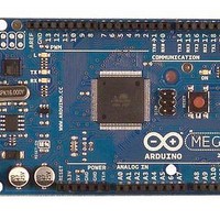
A000047 Arduino, A000047 Datasheet - Page 15
A000047
Manufacturer Part Number
A000047
Description
MCU, MPU & DSP Development Tools Mega2560
Manufacturer
Arduino
Series
-r
Type
MCUr
Specifications of A000047
Processor To Be Evaluated
ATmega2560
Interface Type
USB, I2C, SPI
Dimensions
4 in x 2.1 in
Operating Supply Voltage
5 V
Contents
Board
Lead Free Status / RoHS Status
Lead free / RoHS Compliant
For Use With/related Products
ATmega2560


6.5
6.5.1
2549M–AVR–09/10
General Purpose Register File
The X-register, Y-register, and Z-register
• Bit 0 – C: Carry Flag
The Carry Flag C indicates a carry in an arithmetic or logic operation. See the “Instruction Set
Description” for detailed information.
The Register File is optimized for the AVR Enhanced RISC instruction set. In order to achieve
the required performance and flexibility, the following input/output schemes are supported by the
Register File:
•
•
•
•
Figure 6-2
Figure 6-2.
Most of the instructions operating on the Register File have direct access to all registers, and
most of them are single cycle instructions.
As shown in
directly into the first 32 locations of the user Data Space. Although not being physically imple-
mented as SRAM locations, this memory organization provides great flexibility in access of the
registers, as the X-, Y- and Z-pointer registers can be set to index any register in the file.
The registers R26..R31 have some added functions to their general purpose usage. These reg-
isters are 16-bit address pointers for indirect addressing of the data space. The three indirect
address registers X, Y, and Z are defined as described in
One 8-bit output operand and one 8-bit result input
Two 8-bit output operands and one 8-bit result input
Two 8-bit output operands and one 16-bit result input
One 16-bit output operand and one 16-bit result input
Registers
Purpose
Working
General
shows the structure of the 32 general purpose working registers in the CPU.
Figure
AVR CPU General Purpose Working Registers
6-2, each register is also assigned a data memory address, mapping them
7
ATmega640/1280/1281/2560/2561
R13
R14
R15
R16
R17
R26
R27
R28
R29
R30
R31
R0
R1
R2
…
…
0
Addr.
0x0D
0x0E
0x0F
0x1A
0x1B
0x1C
0x1D
0x1E
0x1F
0x00
0x01
0x02
0x10
0x11
Figure 6-3 on page
X-register High Byte
Y-register High Byte
Z-register High Byte
X-register Low Byte
Y-register Low Byte
Z-register Low Byte
16.
15
Related parts for A000047
Image
Part Number
Description
Manufacturer
Datasheet
Request
R

Part Number:
Description:
Daughter Cards & OEM Boards ARDUINO UNO PROTO PCB REV 3
Manufacturer:
Arduino
Part Number:
Description:
Daughter Cards & OEM Boards ARDUINO SHIELD PROTO KIT REV 3
Manufacturer:
Arduino
Part Number:
Description:
Daughter Cards & OEM Boards ARDUINO MEGA PROTO KIT REV 3
Manufacturer:
Arduino
Part Number:
Description:
Daughter Cards & OEM Boards ARDUINO MEGA PROTO PCB REV 3
Manufacturer:
Arduino
Part Number:
Description:
Development Boards & Kits - AVR ARDUINO STARTER KIT W/ UNO REV3
Manufacturer:
Arduino
Part Number:
Description:
RF Development Tools ARDUINO SHIELD WIRELESS PROTO
Manufacturer:
Arduino
Datasheet:
Part Number:
Description:
RF Development Tools ARDUINO SHIELD WIRELESS WITH SD
Manufacturer:
Arduino
Datasheet:

Part Number:
Description:
Development Software Getting started w/Arduino
Manufacturer:
Arduino

Part Number:
Description:
Ethernet Modules & Development Tools Ethernet Shield for Arduino
Manufacturer:
Arduino

Part Number:
Description:
MCU, MPU & DSP Development Tools LilyPad Arduino Main Board
Manufacturer:
Arduino

Part Number:
Description:
ARDUINO NANO Board
Manufacturer:
Arduino
Datasheet:
Part Number:
Description:
Ethernet Modules & Development Tools ETHERNET SHEILD PoE FOR ARDUINO
Manufacturer:
Arduino
Datasheet:

Part Number:
Description:
ATMEGA328 MCU IC W/ Arduino UNO Bootloader
Manufacturer:
Arduino
Datasheet:
Part Number:
Description:
Memory Cards MICRO SD CARD 1GB WITH SD ADAPTER
Manufacturer:
Arduino