A000047 Arduino, A000047 Datasheet - Page 219
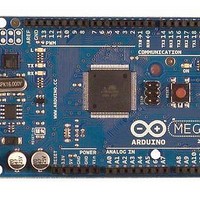
A000047
Manufacturer Part Number
A000047
Description
MCU, MPU & DSP Development Tools Mega2560
Manufacturer
Arduino
Series
-r
Type
MCUr
Specifications of A000047
Processor To Be Evaluated
ATmega2560
Interface Type
USB, I2C, SPI
Dimensions
4 in x 2.1 in
Operating Supply Voltage
5 V
Contents
Board
Lead Free Status / RoHS Status
Lead free / RoHS Compliant
For Use With/related Products
ATmega2560


21.7.2
2549M–AVR–09/10
Asynchronous Data Recovery
Figure 21-5. Start Bit Sampling
When the clock recovery logic detects a high (idle) to low (start) transition on the RxDn line, the
start bit detection sequence is initiated. Let sample 1 denote the first zero-sample as shown in
the figure. The clock recovery logic then uses samples 8, 9, and 10 for Normal mode, and sam-
ples 4, 5, and 6 for Double Speed mode (indicated with sample numbers inside boxes on the
figure), to decide if a valid start bit is received. If two or more of these three samples have logical
high levels (the majority wins), the start bit is rejected as a noise spike and the Receiver starts
looking for the next high to low-transition. If however, a valid start bit is detected, the clock recov-
ery logic is synchronized and the data recovery can begin. The synchronization process is
repeated for each start bit.
When the receiver clock is synchronized to the start bit, the data recovery can begin. The data
recovery unit uses a state machine that has 16 states for each bit in Normal mode and eight
states for each bit in Double Speed mode.
the parity bit. Each of the samples is given a number that is equal to the state of the recovery
unit.
Figure 21-6. Sampling of Data and Parity Bit
The decision of the logic level of the received bit is taken by doing a majority voting of the logic
value to the three samples in the center of the received bit. The center samples are emphasized
on the figure by having the sample number inside boxes. The majority voting process is done as
follows: If two or all three samples have high levels, the received bit is registered to be a logic 1.
If two or all three samples have low levels, the received bit is registered to be a logic 0. This
majority voting process acts as a low pass filter for the incoming signal on the RxDn pin. The
recovery process is then repeated until a complete frame is received. Including the first stop bit.
Note that the Receiver only uses the first stop bit of a frame.
Figure 21-7 on page 220
of the start bit of the next frame.
(U2X = 0)
(U2X = 1)
Sample
Sample
(U2X = 0)
(U2X = 1)
Sample
Sample
RxD
RxD
0
0
IDLE
0
1
1
1
1
shows the sampling of the stop bit and the earliest possible beginning
2
2
3
2
3
2
ATmega640/1280/1281/2560/2561
4
4
5
3
5
3
6
6
Figure 21-6
7
4
7
4
8
8
START
BIT n
9
5
9
5
10
10
shows the sampling of the data bits and
11
11
6
6
12
12
13
13
7
7
14
14
15
15
8
8
16
16
1
1
1
1
2
BIT 0
3
2
219
Related parts for A000047
Image
Part Number
Description
Manufacturer
Datasheet
Request
R

Part Number:
Description:
Daughter Cards & OEM Boards ARDUINO UNO PROTO PCB REV 3
Manufacturer:
Arduino
Part Number:
Description:
Daughter Cards & OEM Boards ARDUINO SHIELD PROTO KIT REV 3
Manufacturer:
Arduino
Part Number:
Description:
Daughter Cards & OEM Boards ARDUINO MEGA PROTO KIT REV 3
Manufacturer:
Arduino
Part Number:
Description:
Daughter Cards & OEM Boards ARDUINO MEGA PROTO PCB REV 3
Manufacturer:
Arduino
Part Number:
Description:
Development Boards & Kits - AVR ARDUINO STARTER KIT W/ UNO REV3
Manufacturer:
Arduino
Part Number:
Description:
RF Development Tools ARDUINO SHIELD WIRELESS PROTO
Manufacturer:
Arduino
Datasheet:
Part Number:
Description:
RF Development Tools ARDUINO SHIELD WIRELESS WITH SD
Manufacturer:
Arduino
Datasheet:

Part Number:
Description:
Development Software Getting started w/Arduino
Manufacturer:
Arduino

Part Number:
Description:
Ethernet Modules & Development Tools Ethernet Shield for Arduino
Manufacturer:
Arduino

Part Number:
Description:
MCU, MPU & DSP Development Tools LilyPad Arduino Main Board
Manufacturer:
Arduino

Part Number:
Description:
ARDUINO NANO Board
Manufacturer:
Arduino
Datasheet:
Part Number:
Description:
Ethernet Modules & Development Tools ETHERNET SHEILD PoE FOR ARDUINO
Manufacturer:
Arduino
Datasheet:

Part Number:
Description:
ATMEGA328 MCU IC W/ Arduino UNO Bootloader
Manufacturer:
Arduino
Datasheet:
Part Number:
Description:
Memory Cards MICRO SD CARD 1GB WITH SD ADAPTER
Manufacturer:
Arduino