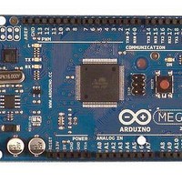
A000047 Arduino, A000047 Datasheet - Page 83
A000047
Manufacturer Part Number
A000047
Description
MCU, MPU & DSP Development Tools Mega2560
Manufacturer
Arduino
Series
-r
Type
MCUr
Specifications of A000047
Processor To Be Evaluated
ATmega2560
Interface Type
USB, I2C, SPI
Dimensions
4 in x 2.1 in
Operating Supply Voltage
5 V
Contents
Board
Lead Free Status / RoHS Status
Lead free / RoHS Compliant
For Use With/related Products
ATmega2560


12.3.4
2549M–AVR–09/10
Alternate Functions of Port D
Table 12-11. Overriding Signals for Alternate Functions in PC3:PC0
The Port D pins with alternate functions are shown in
Table 12-12. Port D Pins Alternate Functions
The alternate pin configuration is as follows:
• T0 – Port D, Bit 7
T0, Timer/Counter0 counter source.
• T1 – Port D, Bit 6
T1, Timer/Counter1 counter source.
• XCK1 – Port D, Bit 5
XCK1, USART1 External clock. The Data Direction Register (DDD5) controls whether the clock
is output (DDD5 set) or input (DDD5 cleared). The XCK1 pin is active only when the USART1
operates in Synchronous mode.
• ICP1 – Port D, Bit 4
ICP1 – Input Capture Pin 1: The PD4 pin can act as an input capture pin for Timer/Counter1.
DIEOE
Signal
DIEOV
DDOE
Name
PUOE
PUOV
DDOV
PVOE
PVOV
Port Pin
AIO
DI
PD7
PD6
PD5
PD4
PD3
PD2
PD1
PD0
SRE • (XMM<5)
SRE • (XMM<5)
SRE • (XMM<5)
PC3/A11
A11
0
1
0
0
–
–
INT3/TXD1 (External Interrupt3 Input or USART1 Transmit Pin)
INT2/RXD1 (External Interrupt2 Input or USART1 Receive Pin)
INT0/SCL (External Interrupt0 Input or TWI Serial CLock)
INT1/SDA (External Interrupt1 Input or TWI Serial DAta)
ATmega640/1280/1281/2560/2561
XCK1 (USART1 External Clock Input/Output)
ICP1 (Timer/Counter1 Input Capture Trigger)
SRE • (XMM<6)
SRE • (XMM<6)
SRE • (XMM<6)
PC2/A10
T0 (Timer/Counter0 Clock Input)
T1 (Timer/Counter1 Clock Input)
A10
0
1
0
0
–
–
Alternate Function
Table
SRE • (XMM<7)
SRE • (XMM<7)
SRE • (XMM<7)
12-12.
PC1/A9
A9
0
1
0
0
–
–
SRE • (XMM<7)
SRE • (XMM<7)
SRE • (XMM<7)
PC0/A8
A8
0
1
0
0
–
–
83
Related parts for A000047
Image
Part Number
Description
Manufacturer
Datasheet
Request
R

Part Number:
Description:
Daughter Cards & OEM Boards ARDUINO UNO PROTO PCB REV 3
Manufacturer:
Arduino
Part Number:
Description:
Daughter Cards & OEM Boards ARDUINO SHIELD PROTO KIT REV 3
Manufacturer:
Arduino
Part Number:
Description:
Daughter Cards & OEM Boards ARDUINO MEGA PROTO KIT REV 3
Manufacturer:
Arduino
Part Number:
Description:
Daughter Cards & OEM Boards ARDUINO MEGA PROTO PCB REV 3
Manufacturer:
Arduino
Part Number:
Description:
Development Boards & Kits - AVR ARDUINO STARTER KIT W/ UNO REV3
Manufacturer:
Arduino
Part Number:
Description:
RF Development Tools ARDUINO SHIELD WIRELESS PROTO
Manufacturer:
Arduino
Datasheet:
Part Number:
Description:
RF Development Tools ARDUINO SHIELD WIRELESS WITH SD
Manufacturer:
Arduino
Datasheet:

Part Number:
Description:
Development Software Getting started w/Arduino
Manufacturer:
Arduino

Part Number:
Description:
Ethernet Modules & Development Tools Ethernet Shield for Arduino
Manufacturer:
Arduino

Part Number:
Description:
MCU, MPU & DSP Development Tools LilyPad Arduino Main Board
Manufacturer:
Arduino

Part Number:
Description:
ARDUINO NANO Board
Manufacturer:
Arduino
Datasheet:
Part Number:
Description:
Ethernet Modules & Development Tools ETHERNET SHEILD PoE FOR ARDUINO
Manufacturer:
Arduino
Datasheet:

Part Number:
Description:
ATMEGA328 MCU IC W/ Arduino UNO Bootloader
Manufacturer:
Arduino
Datasheet:
Part Number:
Description:
Memory Cards MICRO SD CARD 1GB WITH SD ADAPTER
Manufacturer:
Arduino