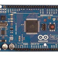
A000047 Arduino, A000047 Datasheet - Page 126
A000047
Manufacturer Part Number
A000047
Description
MCU, MPU & DSP Development Tools Mega2560
Manufacturer
Arduino
Series
-r
Type
MCUr
Specifications of A000047
Processor To Be Evaluated
ATmega2560
Interface Type
USB, I2C, SPI
Dimensions
4 in x 2.1 in
Operating Supply Voltage
5 V
Contents
Board
Lead Free Status / RoHS Status
Lead free / RoHS Compliant
For Use With/related Products
ATmega2560


15.7.4
2549M–AVR–09/10
Phase Correct PWM Mode
The phase correct PWM mode (WGM02:0 = 1 or 5) provides a high resolution phase correct
PWM waveform generation option. The phase correct PWM mode is based on a dual-slope
operation. The counter counts repeatedly from BOTTOM to TOP and then from TOP to BOT-
TOM. TOP is defined as 0xFF when WGM2:0 = 1, and OCR0A when WGM2:0 = 5. In non-
inverting Compare Output mode, the Output Compare (OC0x) is cleared on the Compare Match
between TCNT0 and OCR0x while upcounting, and set on the Compare Match while down-
counting. In inverting Output Compare mode, the operation is inverted. The dual-slope operation
has lower maximum operation frequency than single slope operation. However, due to the sym-
metric feature of the dual-slope PWM modes, these modes are preferred for motor control
applications.
In phase correct PWM mode the counter is incremented until the counter value matches TOP.
When the counter reaches TOP, it changes the count direction. The TCNT0 value will be equal
to TOP for one timer clock cycle. The timing diagram for the phase correct PWM mode is shown
on
the dual-slope operation. The diagram includes non-inverted and inverted PWM outputs. The
small horizontal line marks on the TCNT0 slopes represent Compare Matches between OCR0x
and TCNT0.
Figure 15-7. Phase Correct PWM Mode, Timing Diagram
The Timer/Counter Overflow Flag (TOV0) is set each time the counter reaches BOTTOM. The
Interrupt Flag can be used to generate an interrupt each time the counter reaches the BOTTOM
value.
In phase correct PWM mode, the compare unit allows generation of PWM waveforms on the
OC0x pins. Setting the COM0x1:0 bits to two will produce a non-inverted PWM. An inverted
PWM output can be generated by setting the COM0x1:0 to three: Setting the COM0A0 bits to
one allows the OC0A pin to toggle on Compare Matches if the WGM02 bit is set. This option is
not available for the OC0B pin (see
visible on the port pin if the data direction for the port pin is set as output. The PWM waveform is
Figure
TCNTn
OCnx
OCnx
Period
15-7. The TCNT0 value is in the timing diagram shown as a histogram for illustrating
1
ATmega640/1280/1281/2560/2561
Table 15-4 on page
2
130). The actual OC0x value will only be
3
OCnx Interrupt Flag Set
OCRnx Update
TOVn Interrupt Flag Set
(COMnx1:0 = 2)
(COMnx1:0 = 3)
126
Related parts for A000047
Image
Part Number
Description
Manufacturer
Datasheet
Request
R

Part Number:
Description:
Daughter Cards & OEM Boards ARDUINO UNO PROTO PCB REV 3
Manufacturer:
Arduino
Part Number:
Description:
Daughter Cards & OEM Boards ARDUINO SHIELD PROTO KIT REV 3
Manufacturer:
Arduino
Part Number:
Description:
Daughter Cards & OEM Boards ARDUINO MEGA PROTO KIT REV 3
Manufacturer:
Arduino
Part Number:
Description:
Daughter Cards & OEM Boards ARDUINO MEGA PROTO PCB REV 3
Manufacturer:
Arduino
Part Number:
Description:
Development Boards & Kits - AVR ARDUINO STARTER KIT W/ UNO REV3
Manufacturer:
Arduino
Part Number:
Description:
RF Development Tools ARDUINO SHIELD WIRELESS PROTO
Manufacturer:
Arduino
Datasheet:
Part Number:
Description:
RF Development Tools ARDUINO SHIELD WIRELESS WITH SD
Manufacturer:
Arduino
Datasheet:

Part Number:
Description:
Development Software Getting started w/Arduino
Manufacturer:
Arduino

Part Number:
Description:
Ethernet Modules & Development Tools Ethernet Shield for Arduino
Manufacturer:
Arduino

Part Number:
Description:
MCU, MPU & DSP Development Tools LilyPad Arduino Main Board
Manufacturer:
Arduino

Part Number:
Description:
ARDUINO NANO Board
Manufacturer:
Arduino
Datasheet:
Part Number:
Description:
Ethernet Modules & Development Tools ETHERNET SHEILD PoE FOR ARDUINO
Manufacturer:
Arduino
Datasheet:

Part Number:
Description:
ATMEGA328 MCU IC W/ Arduino UNO Bootloader
Manufacturer:
Arduino
Datasheet:
Part Number:
Description:
Memory Cards MICRO SD CARD 1GB WITH SD ADAPTER
Manufacturer:
Arduino