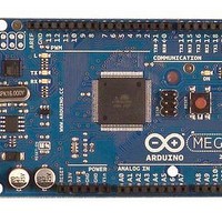
A000047 Arduino, A000047 Datasheet - Page 346
A000047
Manufacturer Part Number
A000047
Description
MCU, MPU & DSP Development Tools Mega2560
Manufacturer
Arduino
Series
-r
Type
MCUr
Specifications of A000047
Processor To Be Evaluated
ATmega2560
Interface Type
USB, I2C, SPI
Dimensions
4 in x 2.1 in
Operating Supply Voltage
5 V
Contents
Board
Lead Free Status / RoHS Status
Lead free / RoHS Compliant
For Use With/related Products
ATmega2560


29.7.11
29.7.12
2549M–AVR–09/10
Programming the Lock Bits
Reading the Fuse and Lock Bits
Figure 29-5. Programming the FUSES Waveforms
The algorithm for programming the Lock bits is as follows (refer to
page 341
1. A: Load Command “0010 0000”.
2. C: Load Data Low Byte. Bit n = “0” programs the Lock bit. If LB mode 3 is programmed
3. Give WR a negative pulse and wait for RDY/BSY to go high.
The Lock bits can only be cleared by executing Chip Erase.
The algorithm for reading the Fuse and Lock bits is as follows (refer to
on page 341
1. A: Load Command “0000 0100”.
2. Set OE to “0”, and BS2, BS1 to “00”. The status of the Fuse Low bits can now be read at
3. Set OE to “0”, and BS2, BS1 to “11”. The status of the Fuse High bits can now be read at
4. Set OE to “0”, and BS2, BS1 to “10”. The status of the Extended Fuse bits can now be
5. Set OE to “0”, and BS2, BS1 to “01”. The status of the Lock bits can now be read at DATA
6. Set OE to “1”.
(LB1 and LB2 is programmed), it is not possible to program the Boot Lock bits by any
External Programming mode.
DATA (“0” means programmed).
DATA (“0” means programmed).
read at DATA (“0” means programmed).
(“0” means programmed).
RESET +12V
RDY/BSY
PAGEL
XTAL1
DATA
for details on Command and Data loading):
XA1
XA0
BS1
BS2
WR
OE
for details on Command loading):
0x40
A
DATA
C
Write Fuse Low byte
XX
ATmega640/1280/1281/2560/2561
0x40
A
DATA
C
Write Fuse high byte
XX
“Programming the Flash” on
0x40
A
“Programming the Flash”
DATA
C
Write Extended Fuse byte
XX
346
Related parts for A000047
Image
Part Number
Description
Manufacturer
Datasheet
Request
R

Part Number:
Description:
Daughter Cards & OEM Boards ARDUINO UNO PROTO PCB REV 3
Manufacturer:
Arduino
Part Number:
Description:
Daughter Cards & OEM Boards ARDUINO SHIELD PROTO KIT REV 3
Manufacturer:
Arduino
Part Number:
Description:
Daughter Cards & OEM Boards ARDUINO MEGA PROTO KIT REV 3
Manufacturer:
Arduino
Part Number:
Description:
Daughter Cards & OEM Boards ARDUINO MEGA PROTO PCB REV 3
Manufacturer:
Arduino
Part Number:
Description:
Development Boards & Kits - AVR ARDUINO STARTER KIT W/ UNO REV3
Manufacturer:
Arduino
Part Number:
Description:
RF Development Tools ARDUINO SHIELD WIRELESS PROTO
Manufacturer:
Arduino
Datasheet:
Part Number:
Description:
RF Development Tools ARDUINO SHIELD WIRELESS WITH SD
Manufacturer:
Arduino
Datasheet:

Part Number:
Description:
Development Software Getting started w/Arduino
Manufacturer:
Arduino

Part Number:
Description:
Ethernet Modules & Development Tools Ethernet Shield for Arduino
Manufacturer:
Arduino

Part Number:
Description:
MCU, MPU & DSP Development Tools LilyPad Arduino Main Board
Manufacturer:
Arduino

Part Number:
Description:
ARDUINO NANO Board
Manufacturer:
Arduino
Datasheet:
Part Number:
Description:
Ethernet Modules & Development Tools ETHERNET SHEILD PoE FOR ARDUINO
Manufacturer:
Arduino
Datasheet:

Part Number:
Description:
ATMEGA328 MCU IC W/ Arduino UNO Bootloader
Manufacturer:
Arduino
Datasheet:
Part Number:
Description:
Memory Cards MICRO SD CARD 1GB WITH SD ADAPTER
Manufacturer:
Arduino