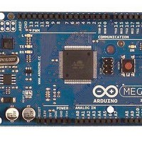
A000047 Arduino, A000047 Datasheet - Page 173
A000047
Manufacturer Part Number
A000047
Description
MCU, MPU & DSP Development Tools Mega2560
Manufacturer
Arduino
Series
-r
Type
MCUr
Specifications of A000047
Processor To Be Evaluated
ATmega2560
Interface Type
USB, I2C, SPI
Dimensions
4 in x 2.1 in
Operating Supply Voltage
5 V
Contents
Board
Lead Free Status / RoHS Status
Lead free / RoHS Compliant
For Use With/related Products
ATmega2560


18.2.1
2549M–AVR–09/10
Timing example
When the modulator is enabled the type of modulation (logical AND or OR) can be selected by
the PORTB7 Register. Note that the DDRB7 controls the direction of the port independent of the
COMnx1:0 bit setting.
Figure 18-3
ate in fast PWM mode (non-inverted) and Timer/Counter0 uses CTC waveform mode with toggle
Compare Output mode (COMnx1:0 = 1).
Figure 18-3. Output Compare Modulator, Timing Diagram
In this example, Timer/Counter2 provides the carrier, while the modulating signal is generated
by the Output Compare unit C of the Timer/Counter1.
The resolution of the PWM signal (OC1C) is reduced by the modulation. The reduction factor is
equal to the number of system clock cycles of one period of the carrier (OC0A). In this example
the resolution is reduced by a factor of two. The reason for the reduction is illustrated in
18-3
high time is one cycle longer than the period 3 high time, but the result on the PB7 output is
equal in both periods.
(FPWM Mode)
(PORTB7 = 0)
(PORTB7 = 1)
(CTC Mode)
(Period)
at the second and third period of the PB7 output when PORTB7 equals zero. The period 2
OC1C
OC0A
clk
PB7
PB7
I/O
illustrates the modulator in action. In this example the Timer/Counter1 is set to oper-
1
ATmega640/1280/1281/2560/2561
2
3
Figure
173
Related parts for A000047
Image
Part Number
Description
Manufacturer
Datasheet
Request
R

Part Number:
Description:
Daughter Cards & OEM Boards ARDUINO UNO PROTO PCB REV 3
Manufacturer:
Arduino
Part Number:
Description:
Daughter Cards & OEM Boards ARDUINO SHIELD PROTO KIT REV 3
Manufacturer:
Arduino
Part Number:
Description:
Daughter Cards & OEM Boards ARDUINO MEGA PROTO KIT REV 3
Manufacturer:
Arduino
Part Number:
Description:
Daughter Cards & OEM Boards ARDUINO MEGA PROTO PCB REV 3
Manufacturer:
Arduino
Part Number:
Description:
Development Boards & Kits - AVR ARDUINO STARTER KIT W/ UNO REV3
Manufacturer:
Arduino
Part Number:
Description:
RF Development Tools ARDUINO SHIELD WIRELESS PROTO
Manufacturer:
Arduino
Datasheet:
Part Number:
Description:
RF Development Tools ARDUINO SHIELD WIRELESS WITH SD
Manufacturer:
Arduino
Datasheet:

Part Number:
Description:
Development Software Getting started w/Arduino
Manufacturer:
Arduino

Part Number:
Description:
Ethernet Modules & Development Tools Ethernet Shield for Arduino
Manufacturer:
Arduino

Part Number:
Description:
MCU, MPU & DSP Development Tools LilyPad Arduino Main Board
Manufacturer:
Arduino

Part Number:
Description:
ARDUINO NANO Board
Manufacturer:
Arduino
Datasheet:
Part Number:
Description:
Ethernet Modules & Development Tools ETHERNET SHEILD PoE FOR ARDUINO
Manufacturer:
Arduino
Datasheet:

Part Number:
Description:
ATMEGA328 MCU IC W/ Arduino UNO Bootloader
Manufacturer:
Arduino
Datasheet:
Part Number:
Description:
Memory Cards MICRO SD CARD 1GB WITH SD ADAPTER
Manufacturer:
Arduino