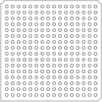
LFXP2-5E-5FTN256I Lattice, LFXP2-5E-5FTN256I Datasheet - Page 135

LFXP2-5E-5FTN256I
Manufacturer Part Number
LFXP2-5E-5FTN256I
Description
FPGA - Field Programmable Gate Array 5K LUTs 172 I/O Inst on DSP 1.2V -5 Spd
Manufacturer
Lattice
Datasheet
1.LFXP2-8E-5FTN256I.pdf
(341 pages)
Specifications of LFXP2-5E-5FTN256I
Number Of Macrocells
5000
Number Of Programmable I/os
172
Data Ram Size
169984
Supply Voltage (max)
1.26 V
Maximum Operating Temperature
+ 100 C
Minimum Operating Temperature
- 40 C
Mounting Style
SMD/SMT
Supply Voltage (min)
1.14 V
Package / Case
FTBGA-256
Number Of Logic Elements/cells
*
Number Of Labs/clbs
*
Total Ram Bits
169984
Number Of I /o
172
Number Of Gates
-
Voltage - Supply
1.14 V ~ 1.26 V
Mounting Type
*
Operating Temperature
-40°C ~ 100°C
Lead Free Status / RoHS Status
Lead free / RoHS Compliant
Available stocks
Company
Part Number
Manufacturer
Quantity
Price
Company:
Part Number:
LFXP2-5E-5FTN256I
Manufacturer:
Lattice
Quantity:
135
Company:
Part Number:
LFXP2-5E-5FTN256I
Manufacturer:
LATTICE
Quantity:
23
Company:
Part Number:
LFXP2-5E-5FTN256I
Manufacturer:
Lattice Semiconductor Corporation
Quantity:
10 000
Part Number:
LFXP2-5E-5FTN256I
Manufacturer:
LATTICE
Quantity:
20 000
- Current page: 135 of 341
- Download datasheet (10Mb)
Table 9-7. User Parameters in the IPexpress GUI (Continued)
Lattice Semiconductor
PLL Modes of Operation
PLLs have many uses within a logic design. The two most popular are Clock Injection Removal and Clock Phase
Adjustment. These two modes of operation are described below.
PLL Clock Injection Removal
In this mode the PLL is used to reduce clock injection delay. Clock injection delay is the delay from the input pin of
the device to a destination element such as a flip-flop. The phase detector of the PLL aligns the CLKI with CLKFB.
If the CLKFB signal comes from the clock tree (CLKOP), then the PLL delay and the clock tree delay is removed.
Figure 9-10 Illustrates an example block diagram and waveform.
CLKOP
CLKOS
CLKOK
CLKOK2
Provide PLL Reset
Provide CLKOK Divide Reset
Provide CLKOS Fine Delay Port
Import LPC to ispLEVER Project
User Parameters
Bypass
Desired Frequency User enters desired CLKOP frequency
Divider
Tolerance
Actual Frequency
Rising
Falling
Delay Multiplier
Enable
Bypass
Phase Shift
Rising
Delay Multiplier
Enable
Bypass
Frequency
Divider
Tolerance
Actual Frequency
Enable
Bypass PLL: CLKOP = CLKI
CLKOP Divider Setting (Divider Mode)
CLKOP tolerance users can tolerate
Actual frequency achievable. Read only
Rising Edge Trim
Falling Edge Trim
Number of delay steps
Enable CLKOS output clock
Bypass PLL: CLKOS = CLKI
CLKOS Static Phase Shift
Rising Edge Trim
Number of Delay steps
Enable CLKOS output clock
Bypass PLL: CLKOK = CLKI
User enters desired CLKOK frequency
CLKOK Divider Setting
CLKOK tolerance users can tolerate
Actual frequency achievable. Read only
Enable CLKOK2 output clock
Provide PLL Reset Port (RESET)
Provide CLKOK Reset Port (RSTK)
Provide CLKOS Fine Delay Port (WRDEL)
Import .lpc file to ispLEVER project
9-13
Description
LatticeXP2 sysCLOCK PLL
Design and Usage Guide
0.0, 0.1, 0.2, 0.5,
0.0, 0.1, 0.2, 0.5,
0.1, 0.2, 0.5, 1.0
0.1, 0.2, 0.5, 1.0
2, 4, 8, 16, 32,
78.125 kHz to
45°..337.5°
217.5 MHz
10 MHz to
48, 64, 80
0°, 22.5°,
435 MHz
ON/OFF
ON/OFF
ON/OFF
ON/OFF
ON/OFF
ON/OFF
ON/OFF
ON/OFF
ON/OFF
ON/OFF
ON/OFF
ON/OFF
ON/OFF
2 to 128
Range
0 to 7
0 to 7
—
—
100 MHz
50 MHz
Default
OFF
OFF
OFF
OFF
OFF
OFF
OFF
OFF
OFF
OFF
OFF
OFF
OFF
0.00
0.0
—
0°
—
8
0
0
2
Related parts for LFXP2-5E-5FTN256I
Image
Part Number
Description
Manufacturer
Datasheet
Request
R

Part Number:
Description:
FPGA - Field Programmable Gate Array 5K LUTs 146I/O Inst- on DSP 1.2V -5 Spd
Manufacturer:
Lattice
Datasheet:

Part Number:
Description:
FPGA - Field Programmable Gate Array 5K LUTs 172I/O Inst- on DSP 1.2V -5 Spd
Manufacturer:
Lattice
Datasheet:

Part Number:
Description:
FPGA - Field Programmable Gate Array 5K LUTs 100 I/O Inst on DSP 1.2V -5 Spd
Manufacturer:
Lattice
Datasheet:

Part Number:
Description:
FPGA - Field Programmable Gate Array 5K LUTs 100I/O Inst- on DSP 1.2V -5 Spd
Manufacturer:
Lattice
Datasheet:
Part Number:
Description:
FPGA LatticeXP2 Family 5000 Cells Flash Technology 1.2V 256-Pin FTBGA
Manufacturer:
LATTICE SEMICONDUCTOR
Datasheet:
Part Number:
Description:
FPGA LatticeXP2 Family 5000 Cells Flash Technology 1.2V 256-Pin FTBGA
Manufacturer:
LATTICE SEMICONDUCTOR
Datasheet:

Part Number:
Description:
IC DSP 5KLUTS 100I/O 144TQFP
Manufacturer:
Lattice
Datasheet:

Part Number:
Description:
IC DSP 5KLUTS 86I/O 132CSBGA
Manufacturer:
Lattice
Datasheet:

Part Number:
Description:
IC DSP 5KLUTS 86I/O 132CSBGA
Manufacturer:
Lattice
Datasheet:

Part Number:
Description:
IC DSP 5KLUTS 146I/O 208PQFP
Manufacturer:
Lattice
Datasheet:

Part Number:
Description:
IC DSP 5KLUTS 146I/O 208PQFP
Manufacturer:
Lattice
Datasheet:

Part Number:
Description:
IC DSP 5KLUTS 172I/O 256FTBGA
Manufacturer:
Lattice
Datasheet:

Part Number:
Description:
IC FPGA 5KLUTS 86I/O 132-BGA
Manufacturer:
Lattice
Datasheet:

Part Number:
Description:
IC FPGA 5KLUTS 86I/O 132-BGA
Manufacturer:
Lattice
Datasheet:

Part Number:
Description:
IC FPGA 5KLUTS 86I/O 132-BGA
Manufacturer:
Lattice
Datasheet:


