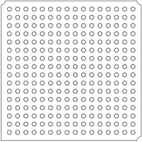
LFXP2-5E-5FTN256I Lattice, LFXP2-5E-5FTN256I Datasheet - Page 330

LFXP2-5E-5FTN256I
Manufacturer Part Number
LFXP2-5E-5FTN256I
Description
FPGA - Field Programmable Gate Array 5K LUTs 172 I/O Inst on DSP 1.2V -5 Spd
Manufacturer
Lattice
Datasheet
1.LFXP2-8E-5FTN256I.pdf
(341 pages)
Specifications of LFXP2-5E-5FTN256I
Number Of Macrocells
5000
Number Of Programmable I/os
172
Data Ram Size
169984
Supply Voltage (max)
1.26 V
Maximum Operating Temperature
+ 100 C
Minimum Operating Temperature
- 40 C
Mounting Style
SMD/SMT
Supply Voltage (min)
1.14 V
Package / Case
FTBGA-256
Number Of Logic Elements/cells
*
Number Of Labs/clbs
*
Total Ram Bits
169984
Number Of I /o
172
Number Of Gates
-
Voltage - Supply
1.14 V ~ 1.26 V
Mounting Type
*
Operating Temperature
-40°C ~ 100°C
Lead Free Status / RoHS Status
Lead free / RoHS Compliant
Available stocks
Company
Part Number
Manufacturer
Quantity
Price
Company:
Part Number:
LFXP2-5E-5FTN256I
Manufacturer:
Lattice
Quantity:
135
Company:
Part Number:
LFXP2-5E-5FTN256I
Manufacturer:
LATTICE
Quantity:
23
Company:
Part Number:
LFXP2-5E-5FTN256I
Manufacturer:
Lattice Semiconductor Corporation
Quantity:
10 000
Part Number:
LFXP2-5E-5FTN256I
Manufacturer:
LATTICE
Quantity:
20 000
- Current page: 330 of 341
- Download datasheet (10Mb)
Lattice Semiconductor
Part 2: Program the Primary Pattern into LatticeXP2 Embedded Flash
Follow the procedures shown in Figure 17-3 and Table 17-5 too program the JEDEC file into the LatticeXP2
embedded Flash using the ispVM System. There is absolutely no difference between programming the LatticeXP2
device for standard single boot and dual boot applications.
For live field upgrade of a mission critical application, Background Mode programming is strongly recommended.
For more details on Background Mode programming mode for mission critical application, please refer to the
LatticeXP2 Mission Critical Field Upgrade Usage Guide. Contact Lattice Applications for the document if required.
Once the embedded Flash and Done fuse is programmed, it can be difficult to configure the LatticeXP2 device from
the external SPI Flash device. There are two methods that can be used to test the dual boot feature does work.
Figure 17-3. Using ispVM to Program a JEDEC into the Embedded Flash
1. Drive the CFG1 pin to 0. This will cause the bitstream in the SPI Flash to be the Primary pattern.
2. Use the ERASE_DONE command to erase only the Done fuse of the LatticeXP2 Embedded Flash. The
only draw back of this approach is that entire LatticeXP2 Embedded Flash will need to be re-programmed.
Simply programming the Done fuse will not work.
6
6 6
2
2 2
3
3 3
4
4 4
1
1 1
17-12
7
7 7
5
5 5
Operation List of Interest
Operation List of Interest
FLASH Erase,Program,Verify,Secure
FLASH Erase,Program,Verify,Secure
FLASH Erase,Program,Verify,Secure
FLASH Erase,Program,Verify,Refresh
FLASH Erase,Program,Verify,Refresh
FLASH Erase,Program,Verify,Refresh
FLASH Verify Only
FLASH Verify Only
FLASH Verify Only
FLASH Erase Only
FLASH Erase Only
FLASH Erase Only
FLASH Read Status Register
FLASH Read Status Register
FLASH Read Status Register
FLASH Read DONE bit
FLASH Read DONE bit
FLASH Read DONE bit
FLASH Refresh
FLASH Refresh
FLASH Refresh
FLASH Erase,Program,Verify
FLASH Erase,Program,Verify
FLASH Erase,Program,Verify
LatticeXP2 Dual Boot Feature
Related parts for LFXP2-5E-5FTN256I
Image
Part Number
Description
Manufacturer
Datasheet
Request
R

Part Number:
Description:
FPGA - Field Programmable Gate Array 5K LUTs 146I/O Inst- on DSP 1.2V -5 Spd
Manufacturer:
Lattice
Datasheet:

Part Number:
Description:
FPGA - Field Programmable Gate Array 5K LUTs 172I/O Inst- on DSP 1.2V -5 Spd
Manufacturer:
Lattice
Datasheet:

Part Number:
Description:
FPGA - Field Programmable Gate Array 5K LUTs 100 I/O Inst on DSP 1.2V -5 Spd
Manufacturer:
Lattice
Datasheet:

Part Number:
Description:
FPGA - Field Programmable Gate Array 5K LUTs 100I/O Inst- on DSP 1.2V -5 Spd
Manufacturer:
Lattice
Datasheet:
Part Number:
Description:
FPGA LatticeXP2 Family 5000 Cells Flash Technology 1.2V 256-Pin FTBGA
Manufacturer:
LATTICE SEMICONDUCTOR
Datasheet:
Part Number:
Description:
FPGA LatticeXP2 Family 5000 Cells Flash Technology 1.2V 256-Pin FTBGA
Manufacturer:
LATTICE SEMICONDUCTOR
Datasheet:

Part Number:
Description:
IC DSP 5KLUTS 100I/O 144TQFP
Manufacturer:
Lattice
Datasheet:

Part Number:
Description:
IC DSP 5KLUTS 86I/O 132CSBGA
Manufacturer:
Lattice
Datasheet:

Part Number:
Description:
IC DSP 5KLUTS 86I/O 132CSBGA
Manufacturer:
Lattice
Datasheet:

Part Number:
Description:
IC DSP 5KLUTS 146I/O 208PQFP
Manufacturer:
Lattice
Datasheet:

Part Number:
Description:
IC DSP 5KLUTS 146I/O 208PQFP
Manufacturer:
Lattice
Datasheet:

Part Number:
Description:
IC DSP 5KLUTS 172I/O 256FTBGA
Manufacturer:
Lattice
Datasheet:

Part Number:
Description:
IC FPGA 5KLUTS 86I/O 132-BGA
Manufacturer:
Lattice
Datasheet:

Part Number:
Description:
IC FPGA 5KLUTS 86I/O 132-BGA
Manufacturer:
Lattice
Datasheet:

Part Number:
Description:
IC FPGA 5KLUTS 86I/O 132-BGA
Manufacturer:
Lattice
Datasheet:


