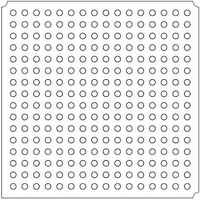
LFXP2-5E-5FTN256I Lattice, LFXP2-5E-5FTN256I Datasheet - Page 185

LFXP2-5E-5FTN256I
Manufacturer Part Number
LFXP2-5E-5FTN256I
Description
FPGA - Field Programmable Gate Array 5K LUTs 172 I/O Inst on DSP 1.2V -5 Spd
Manufacturer
Lattice
Datasheet
1.LFXP2-8E-5FTN256I.pdf
(341 pages)
Specifications of LFXP2-5E-5FTN256I
Number Of Macrocells
5000
Number Of Programmable I/os
172
Data Ram Size
169984
Supply Voltage (max)
1.26 V
Maximum Operating Temperature
+ 100 C
Minimum Operating Temperature
- 40 C
Mounting Style
SMD/SMT
Supply Voltage (min)
1.14 V
Package / Case
FTBGA-256
Number Of Logic Elements/cells
*
Number Of Labs/clbs
*
Total Ram Bits
169984
Number Of I /o
172
Number Of Gates
-
Voltage - Supply
1.14 V ~ 1.26 V
Mounting Type
*
Operating Temperature
-40°C ~ 100°C
Lead Free Status / RoHS Status
Lead free / RoHS Compliant
Available stocks
Company
Part Number
Manufacturer
Quantity
Price
Company:
Part Number:
LFXP2-5E-5FTN256I
Manufacturer:
Lattice
Quantity:
135
Company:
Part Number:
LFXP2-5E-5FTN256I
Manufacturer:
LATTICE
Quantity:
23
Company:
Part Number:
LFXP2-5E-5FTN256I
Manufacturer:
Lattice Semiconductor Corporation
Quantity:
10 000
Part Number:
LFXP2-5E-5FTN256I
Manufacturer:
LATTICE
Quantity:
20 000
- Current page: 185 of 341
- Download datasheet (10Mb)
Lattice Semiconductor
Distributed Single Port RAM (Distributed_SPRAM) – PFU Based
PFU-based Distributed Single Port RAM is created using the 4-input LUT (Look-Up Table) available in the PFU.
These LUTs can be cascaded to create larger Distributed Memory sizes.
Figure 10-39 shows the Distributed Single Port RAM module as generated by IPexpress.
Figure 10-39. Distributed Single Port RAM Module Generated by IPexpress
The generated module makes use 4-input LUT available in the PFU. Additional logic like Clock, Reset is generated
by utilizing the resources available in the PFU.
Ports such as Read Clock (RdClock) and Read Clock Enable (RdClockEn), are not available in the hardware prim-
itive. These are generated by IPexpress when the user wants the to enable the output registers in their IPexpress
configuration.
The various ports and their definitions for the memory are as per Table 10-14. The table lists the corresponding
ports for the module generated by IPexpress and for the primitive.
Table 10-14. PFU-based Distributed Single Port RAM Port Definitions
Ports such as Clock Enable (ClockEn) are not available in the hardware primitive. These are generated by IPex-
press when the user wishes to enable the output registers in the IPexpress configuration.
Users have the option of enabling the output registers for Distributed Single Port RAM (Distributed_SPRAM). Fig-
ures 10-40 and 10-41 show the internal timing waveforms for the Distributed Single Port RAM
(Distributed_SPRAM) with these options.
Generated Module
Port Name in
ClockEn
Address
Reset
Clock
Data
WE
Q
ClockEn
Address
Reset
Clock
Port Name in the
Data
WE
PFU Primitive
DO[1:0]
AD[3:0]
DI[1:0]
WRE
CK
—
—
Distributed Single Port
10-35
PFU based
Memory
Clock Enable
Write Enable
Description
Data Out
Address
Data In
Reset
Clock
LatticeXP2 Memory Usage Guide
Q
Rising Clock Edge
Active State
Active High
Active High
Active High
—
—
—
Related parts for LFXP2-5E-5FTN256I
Image
Part Number
Description
Manufacturer
Datasheet
Request
R

Part Number:
Description:
FPGA - Field Programmable Gate Array 5K LUTs 146I/O Inst- on DSP 1.2V -5 Spd
Manufacturer:
Lattice
Datasheet:

Part Number:
Description:
FPGA - Field Programmable Gate Array 5K LUTs 172I/O Inst- on DSP 1.2V -5 Spd
Manufacturer:
Lattice
Datasheet:

Part Number:
Description:
FPGA - Field Programmable Gate Array 5K LUTs 100 I/O Inst on DSP 1.2V -5 Spd
Manufacturer:
Lattice
Datasheet:

Part Number:
Description:
FPGA - Field Programmable Gate Array 5K LUTs 100I/O Inst- on DSP 1.2V -5 Spd
Manufacturer:
Lattice
Datasheet:
Part Number:
Description:
FPGA LatticeXP2 Family 5000 Cells Flash Technology 1.2V 256-Pin FTBGA
Manufacturer:
LATTICE SEMICONDUCTOR
Datasheet:
Part Number:
Description:
FPGA LatticeXP2 Family 5000 Cells Flash Technology 1.2V 256-Pin FTBGA
Manufacturer:
LATTICE SEMICONDUCTOR
Datasheet:

Part Number:
Description:
IC DSP 5KLUTS 100I/O 144TQFP
Manufacturer:
Lattice
Datasheet:

Part Number:
Description:
IC DSP 5KLUTS 86I/O 132CSBGA
Manufacturer:
Lattice
Datasheet:

Part Number:
Description:
IC DSP 5KLUTS 86I/O 132CSBGA
Manufacturer:
Lattice
Datasheet:

Part Number:
Description:
IC DSP 5KLUTS 146I/O 208PQFP
Manufacturer:
Lattice
Datasheet:

Part Number:
Description:
IC DSP 5KLUTS 146I/O 208PQFP
Manufacturer:
Lattice
Datasheet:

Part Number:
Description:
IC DSP 5KLUTS 172I/O 256FTBGA
Manufacturer:
Lattice
Datasheet:

Part Number:
Description:
IC FPGA 5KLUTS 86I/O 132-BGA
Manufacturer:
Lattice
Datasheet:

Part Number:
Description:
IC FPGA 5KLUTS 86I/O 132-BGA
Manufacturer:
Lattice
Datasheet:

Part Number:
Description:
IC FPGA 5KLUTS 86I/O 132-BGA
Manufacturer:
Lattice
Datasheet:


