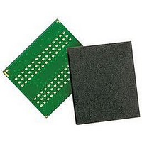
M52S128324A-7BG ELITE SEMICONDUCTOR, M52S128324A-7BG Datasheet - Page 11

M52S128324A-7BG
Manufacturer Part Number
M52S128324A-7BG
Description
IC, SDRAM, 128MBIT, 143MHZ, FBGA-90
Manufacturer
ELITE SEMICONDUCTOR
Datasheet
1.M52S128324A-7BG.pdf
(47 pages)
Specifications of M52S128324A-7BG
Memory Type
DRAM - Sychronous
Memory Configuration
2M X 16
Ic Interface Type
Parallel
Memory Case Style
FBGA
No. Of Pins
90
Operating Temperature Range
0°C To +70°C
Frequency
133MHz
Filter Terminals
SMD
Rohs Compliant
Yes
Page Size
128MB
Lead Free Status / RoHS Status
Lead free / RoHS Compliant
ESMT
MODE REGISTER FIELD TABLE TO PROGRAM MODES
Register Programmed with MRS
POWER UP SEQUENCE
1.Apply power and start clock, Attempt to maintain CKE = ”H”, DQM = ”H” and the other pin are NOP condition at the inputs.
2. Maintain stable power , stable clock and NOP input condition for a minimum of 200us.
3. Issue precharge commands for all banks of the devices.
4. Issue 2 or more auto-refresh commands.
5. Issue mode register set command to initialize the mode register.
cf.) Sequence of 4 & 5 is regardless of the order.
The device is now ready for normal operation.
Note :
Elite Semiconductor Memory Technology Inc.
Function
Address
A8
A9
0
0
1
1
0
1
Write Burst Length
A7
5.During burst read or write with auto precharge. new read/write command can not be issued.
6.Burst stop command is valid at every burst length.
7.DQM sampled at positive going edge of a CLK and masks the data-in at the very CLK (write DQM latency is 0), but
1. RFU(Reserved for future use) should stay “0” during MRS cycle.
2. If A9 is high during MRS cycle, “ Burst Read single Bit Write” function will be enabled.
3. The full column burst (256 bit) is available only at sequential mode of burst type.
0
1
0
1
If both BA1 is “High” and BA0 is “Low” at read ,write , row active and precharge ,bank C is selected.
If both BA1 and BA0 are “High” at read ,write , row active and precharge ,bank D is selected
If A10/AP is “High” at row precharge , BA1 and BA0 is ignored and all banks are selected.
Another bank read/write command can be issued after the end of burst.
New row active of the associated bank can be issued at t
makes Hi-Z state the data-out of 2 CLK cycles after.(Read DQM latency is 2)
Test Mode
Mode Register Set
Single Bit
RFU
A11
Length
Burst
Reserved
Reserved
Reserved
Type
BA0~BA1
RFU
A6
0
0
0
0
1
1
1
1
A5
CAS Latency
A10/AP
0
0
1
1
0
0
1
1
RFU
A4
0
1
0
1
0
1
0
1
Reserved
Reserved
Reserved
Reserved
Reserved
Latency
W.B.L
1
2
3
A9
RP
A3
after the end of burst.
A8
0
1
Burst Type
TM
Sequential
Interleave
A7
Type
A6
CAS Latency
Full Page Length : 256
A2
0
0
0
0
1
1
1
1
A5
Publication Date: Mar. 2008
Revision: 1.3
A1
M52S128324A
0
0
1
0
0
1
1
1
A4
Burst Length
A0
0
1
0
1
0
1
0
1
A3
BT
Reserved Reserved
Reserved Reserved
Reserved Reserved
Full Page Reserved
BT = 0
A2
1
2
4
8
Burst Length
11/47
A1
BT = 1
1
2
4
8
A0


