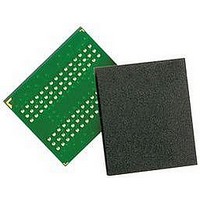
M52S128324A-7BG ELITE SEMICONDUCTOR, M52S128324A-7BG Datasheet - Page 17

M52S128324A-7BG
Manufacturer Part Number
M52S128324A-7BG
Description
IC, SDRAM, 128MBIT, 143MHZ, FBGA-90
Manufacturer
ELITE SEMICONDUCTOR
Datasheet
1.M52S128324A-7BG.pdf
(47 pages)
Specifications of M52S128324A-7BG
Memory Type
DRAM - Sychronous
Memory Configuration
2M X 16
Ic Interface Type
Parallel
Memory Case Style
FBGA
No. Of Pins
90
Operating Temperature Range
0°C To +70°C
Frequency
133MHz
Filter Terminals
SMD
Rohs Compliant
Yes
Page Size
128MB
Lead Free Status / RoHS Status
Lead free / RoHS Compliant
ESMT
Write command
address given by the column address to begin the burst write operation. The first
write data in burst can be input with this command with subsequent data on following
clocks.
Read command
CBR (auto) refresh command
address is generated internally.
row activate command.
M52S128324A cannot accept any other command.
Elite Semiconductor Memory Technology Inc.
If the mode register is in the burst write mode, this command sets the burst start
Read data is available after CAS latency requirements have been met.
This command sets the burst start address given by the column address.
This command is a request to begin the CBR refresh operation. The refresh
Before executing CBR refresh, all banks must be precharged.
After this cycle, all banks will be in the idle (precharged) state and ready for a
During t
( CS , CAS , WE = Low, RAS = High)
( CS , CAS = Low, RAS , WE = High)
( CS , RAS , CAS = Low, WE , CKE = High)
RC
period (from refresh command to refresh or activate command), the
BA0, BA1
(Bank select)
Publication Date: Mar. 2008
Revision: 1.3
BA0, BA1
(Bank select)
BA0, BA1
(Bank select)
Fig. 6 Auto refresh command
Fig. 4 Column address and
RAS
CAS
CLK
RAS
CLK
CKE
CAS
M52S128324A
RAS
Add
WE
CAS
Fig. 5 Column address and
A10
Add
A10
Add
CKE
WE
CKE
CLK
CS
CS
WE
CS
A10
write command
read command
H
H
H
Col.
Col.
17/47


