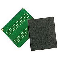
M52S128324A-7BG ELITE SEMICONDUCTOR, M52S128324A-7BG Datasheet - Page 4

M52S128324A-7BG
Manufacturer Part Number
M52S128324A-7BG
Description
IC, SDRAM, 128MBIT, 143MHZ, FBGA-90
Manufacturer
ELITE SEMICONDUCTOR
Datasheet
1.M52S128324A-7BG.pdf
(47 pages)
Specifications of M52S128324A-7BG
Memory Type
DRAM - Sychronous
Memory Configuration
2M X 16
Ic Interface Type
Parallel
Memory Case Style
FBGA
No. Of Pins
90
Operating Temperature Range
0°C To +70°C
Frequency
133MHz
Filter Terminals
SMD
Rohs Compliant
Yes
Page Size
128MB
Lead Free Status / RoHS Status
Lead free / RoHS Compliant
ESMT
BLOCK DIAGRAM
PIN DESCRIPTION
Elite Semiconductor Memory Technology Inc.
CLK
CKE
A0 ~ A11
BA0 , BA1
CS
RAS
CAS
WE
Address
CLK
CKE
CS
RAS
CAS
WE
PIN
Generator
Clock
System Clock
Chip Select
Clock Enable
Address
Bank Select Address
Row Address Strobe
Column Address Strobe
Write Enable
NAME
Register
Mode
Address
Refresh
Counter
Column
Address
Buffer
Refresh
Counter
Buffer
Row
&
&
Active on the positive going edge to sample all inputs
Disables or enables device operation by masking or enabling all
inputs except CLK , CKE and DQM0-3.
Masks system clock to freeze operation from the next clock cycle.
CKE should be enabled at least one cycle prior new command.
Disable input buffers for power down in standby.
Row / column address are multiplexed on the same pins.
Row address : RA0~RA11, column address : CA0~CA7
Selects bank to be activated during row address latch time.
Selects bank for read / write during column address latch time.
Latches row addresses on the positive going edge of the CLK with
Enables row access & precharge.
Latches column address on the positive going edge of the CLK with
Enables column access.
Enables write operation and row precharge.
Latches data in starting from CAS , WE active.
RAS low.
CAS low.
Data Control Circuit
Column Decoder
Sense Amplifier
Bank A
INPUT FUNCTION
Bank B
Bank C
Bank D
Publication Date: Mar. 2008
Revision: 1.3
M52S128324A
DQM0~3
4/47
DQ


